Other Parts Discussed in Thread: UCC28180, UCC28019, TIDA-00443
How to design boost follower circuit with UCC28019AD
This thread has been locked.
If you have a related question, please click the "Ask a related question" button in the top right corner. The newly created question will be automatically linked to this question.
How to design boost follower circuit with UCC28019AD
Hi Sagneetha,
The best example I can provide you is a reference design using the UCC28180 in boost-follower mode. The UCC28180 is similar to the UCC28019. Note the "Boost Follower" circuit block in the schematic which influences VSENSE based on line voltage.
Thank you sir ... in this design does the resistors R1 and R2 are same as of RFB1 and RFB2? which design steps should I follow for this divider network as it may change the over voltage and under voltage setpoints
Hi Sangeetha, If you are referring to Rbf1 & Rfb2 from the UCC28019 datasheet, then Rfb1 is R6+R7+R8 and Rfb2 is R9 in TIDA-00443. Note that the voltage follower circuit uses similar values as the output voltage sense.
*Corrected to reference IDDA-00443 design guide: I have no experience with this boost-follower design, however, I would follow the design procedure on p20 of the TIDA-00443 Design Guide. Since Vout, OVP and UVD are all based on VSENSE, the levels will track proportionally.
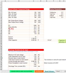
As per design guide for TIDA-00443, in the voltage follower circuit design(page no. 20) why the reference voltage is taken as 5V corresponding to the Vout(min)?
In the calculation of R2 (equation no. 54) why a factor 2 is multiplied?
Hi Sangeetha,
5V is the reference of the voltage error amplifier inside the UCC28180 controller.
The 2 is not a factor, but the design target for the minimum voltage on the base of the NPN transistor (2V). The target maximum is 3V.
Hi sir,
If we take 5V corresponding to minimum Vout, the Pin voltage will be higher for Vout(max) which may exceed the over voltage detection point.. how to take this point into account while designing?
it is mentioned in the document that base voltage of transistor is set according to the voltage divider formed by R3 & R4. Then how R2 is related with this factor? (since R2 is included the divider network for the Vout point only)
Design for 5.0V at VSENSE at low Vin/Vout. OVP/UVP occurs when VSENSE ~4.75V/5.25V (refer to datasheet for more details). The the boost follower circuit modifies the voltage seen at VSENSE in proportion to VIN, so that as Vin increases, the divider voltage will be lowered proportionally to account for the rise in Vout. You should download the Design Guide and Calculation Tool for TIDA-00443 to help you chose the correct values.
R2 is the lower resistor of the Vout divider. R1/R2 ratio is chosen to set VSENSE = 5V at the desired Vout. Without any boost follower circuitry, this would maintain a constant Vout with varying Vin as the controller regulates around this 5V. With the boost-follower connected, the voltage on the high side of R2 is lowered in proportion to increase in Vin (and hence, Vout) to maintain ~5V on VSENSE.
Please read through the documentation completely before you begin your design.
Also note a typographical error in the calculation tool (circled where R2 should be R5).
