A related question is a question created from another question. When the related question is created, it will be automatically linked to the original question.
If you have a related question, please click the "Ask a related question" button in the top right corner. The newly created question will be automatically linked to this question.
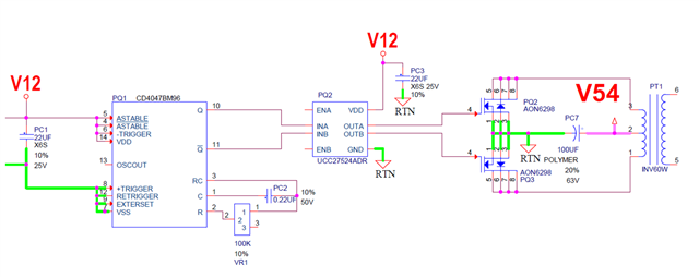
1) Consider putting gate resistors, or at a minimum, gate resistor place holder of 0Ohm short. Otherwise, consider a gate resistor between 1 Ohm to 10 Ohm. This will help reduce power dissipation within the driver, but will slightly increase rise and fall times on the gate drive signals.
2) The VDD bypass capacitor is a bit large, consider using a 4.7uF capacitor instead, and please make sure to place it as close as possible to the VDD and GND pins. If your system is very noisy, consider also populating a 0.1uF capacitor in parallel to the 4.7uF cap, and make sure the 0.1uF is the capacitor closer to the IC.
3) Make sure your oscillator has some built in deadtime to minimize the chance of both MOSFETs being on at the same time, unless this is not a concern to you.
4) It is not needed (because they are internally pulled up), but I suggest tying ENA and ENB to VDD to minimize any chance of unwanted signals getting coupled to either of the ENABLE pins.
5) If you are not going to use gate resistors, consider putting snubbers on your MOSFETs to minimize noise that could be coupled back to the gate driver and/or to the rest of the system.
6) If you are worried about the MOSFETs potentially turning on when the system is in between powering up or off, consider putting a gate-to-source resistor of around 10 kOhm on each of the MOSFETs.
-------
I hope this answers your questions! If so, please press the green button.
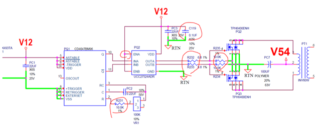
The changes look good. The placeholders for gate resistors and VGS snubbers often come in handy if any issues arise, and they help in testing. We are the gate drivers team, so I think you may also want to post this same question to the group that handles the CD4047 part. I think they would be able to tell you if the implementation of that part is good better than we can.
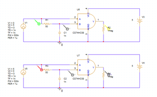
This dead-time circuit seems okay. It is essentially the same thing as this integrated solution. I just want to share the more integrated solution in case you are interested. Here is my schematic:
In this case, the pulses are Q & ~Q with no dead-time. I wasn't 100% on your voltage levels and frequency but this works regardless. Also, you can buy AND gates with multiple gates in one package so think of it as one IC. This circuit works by taking the AND of the signal and a delayed version of itself (much like your discrete solution). This means that the rise time of the RC filter determines the dead-time.
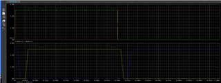
You can see that there is no dead-time between the two input signals, but both outputs have a dead-time configured by the RC filter. Let me know if you are interested in pursuing such a design, and I (or the logic team) can help you implement it. I think it will likely come down to cost/supply of buying the FETs or the IC, since they work in similar ways.