This thread has been locked.

If you have a related question, please click the "Ask a related question" button in the top right corner. The newly created question will be automatically linked to this question.

TLV755P: Output Not Stable (X2SON package)

Part Number: TLV755P
Other Parts Discussed in Thread: TPS7A20, TPS7A02, TLV755

Hello,

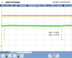
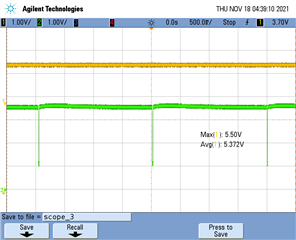
My TLV755P (500mA, 3V LDO, X2SON 1x1mm package) is not stable when driving my ASIC*. My ASIC has already been tested to be working fine with e.g. the LT3021 (https://www.analog.com/en/products/lt3021.html). Every ~300 milliseconds or so, the output dips down to ~1V for ~10 milliseconds. Actually, we also originally tried the TPS7A02 3.3V and TPS7A20 3.6V X2SON LDOs but they also exhibited this dipping phenomenon.

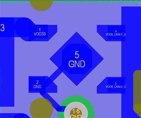
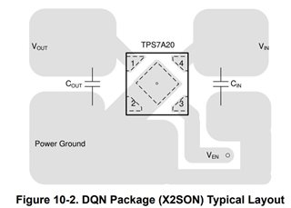
*I have tried input caps {1u, 1u} and {1u, 1u, 10u} as well as output caps {0.1u, 1u} and {0.1u, 1u, 10u} which have all been placed close to TLV55P on the PCB. The ASIC includes 3x additional LDOs which drive digital logic, and a few other analog circuits. Also, the X2SON packages have been reflow soldered, once by another company, and once by myself.

Is there some instability in my circuit? Has this occurred for others before? 

Thank you for your time,

Nate

  • I should note that in my design, there are 2x TPS7A20 1.8V LDOs which drive different circuitry next to the TLV755P LDO. These two are working fine.

    Nate

  • Hi Nathan,

    This behavior does not sound like a stability problem, but if you can provide scope shots it will be easy to tell. Please include Vin, Vout, and if possible Iin or Iout.

    Regards,

    Nick

  • Hi Nick,

    I figured out that the TLV755 works OK if I reduce the input voltage to ~5.1V. But if I increase to ~5.3V then it becomes "unstable" --see scope shots of input voltage (yellow) and output voltage (green) here:

    https://drive.google.com/drive/folders/1pKch2uRxDCMOlFJmxdMs9EydkvzgTUwp?usp=sharing

    Let me know if you can't see anything. Unfortunately, there's no easy way to measure input/output current because the X2SON package is very small (1x1mm surface mount, like a dust particle). However, I am able to see that the DC current consumption from my power supply is ~234mA. 

    Why does the output fluctuate when the operating conditions are within spec (< 500 mA current, < 5.5V input voltage)?

    Thanks,

    Nate

  • Hi Nathan,

    I can't access the drive for security reasons. Can you post the scope shots here directly?

    Regards,

    Nick

  • How? The Image/video/file option asks for a file/URL in text format. I entered the location of the file on my desktop but it's not working. Please advise.

    Nate

  • The forums were updated somewhat recently to allow you to directly paste images into the text box to embed them. I've seen videos embedded directly as well but I haven't done it myself.

  • Oh, I see now. I didn't realize the "Upload" text was selectable. Here you go:

    Nate

  • That looks to me like it's going into thermal shutdown briefly. What is the input and output voltages and the output current? Also are you testing this at room temp?

  • Ahh, thermal shutdown would make sense, as the part gets quite hot (the PCB is quite small, ~20x30mm), and I think my layout wasn't great because the thermal resistance is too high between the X2SON ground pad and the PCB ground:

    I have had difficulty in the past with reflow soldering of QFN packages where solder beneath the central ground pad wouldn't melt because the thermal resistance to the ground plane was too low. Here it seems I have gone too far in the opposite direction, and should have followed the recommended layout guideline in the first place:

    Anyway, to answer your question: Input is yellow (either 5.1 or 5.3V) while output is green (~3.6V). I have no way to measure in/out current, but my power supply is reading 234 mA of current. Yes, this is tested at room temperature.

    Also, it seems those captures were with the TPSA720 (3.6V) (Actually, this was the part we wanted to use, but I could not find TPS7A20 when I created this post in the forum). 

    If you have more suggestions please let me know, otherwise I will mark this as resolved.

    Thanks!

    Nate

  • Hi Nate,

    Yeah, assuming all 234mA of that current is going through the LDO, that is about (5.1V - 3.6V) * .234A = 351mW, and this would correspond to (using the datasheet specs) a junction temperature rise of 351mW * 166.1C/W = 58C. This would not be too much of an issue at room temp if there were thermal vias underneath the thermal pad because the thermal metrics are simulated assuming there are thermal vias, but unfortunately the thermal performance of your layout is likely worse than the datasheet specs. So, my recommendation would be to connect the thermal pad to more top-layer copper and/or add thermal vias underneath the thermal pad. With these changes I think the part will not enter thermal shutdown (again assuming that your actual application is also at room temp).

    Regards,

    Nick

  • Thanks a lot for your help. (The application is at room temp).

    Nate