This thread has been locked.

If you have a related question, please click the "Ask a related question" button in the top right corner. The newly created question will be automatically linked to this question.

LM22678: We have design Switcher using LM22678J-5 V For 5A we need help for Switcher to remove output voltage noise

Part Number: LM22678

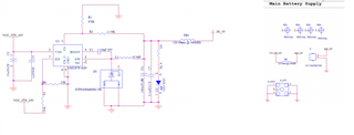
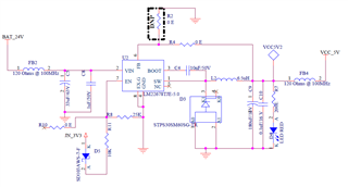
  this is my schematic of lm22678 in which i get output voltage with noise .

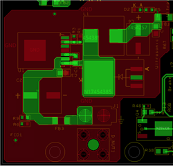
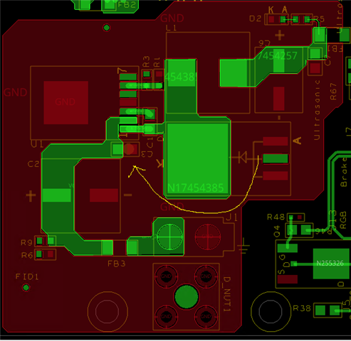
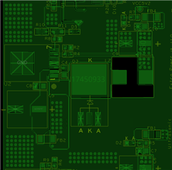
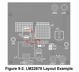
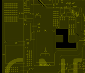
   this is top and bottom layer of my design receptively .

   and this is dso result of switcher output voltage. please give some solution to reduce noise.

  • HI

    1. follow the layout guild line(Datasheet section9.1), I can't find how the diode GND go back to C8 GND which is input ceramic cap.

    2. add more ceramic capacitor at output side to see whether it is helpful

    3. test SW waveform, see the overshoot spike, adding the snubber to see whether the spike reduce. and also pls pay attention to the power loss of snubber.

  • Hello Daniel, thanks for reply.

    Please check below image of the layout photo where GND between C8 and diode connect at same layer.

    meanwhile i will test option 2 and option3

    Please note :- we are going to update this PCB you can let us know if there any change required.

  • Hi

    It is in same layer, but how the red line go to the C8 GND?

    from datasheet example, we can see it has very small loop area from CAP VIN->IC  Vin pin->IC SW->DIODE SW->DIODE GND->CAP GND

  • datasheet

    Thank you for your reply. 

    C8 capacitor GND and Vin path shown as below image


    also please note:


    while i measured output voltage across output filter capacitor C9 i got noiseless output but when i  change  capacitor ground with common ground i got noise . DSO output image shared below please check 

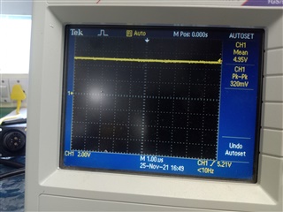
     output across C9 capacitor.

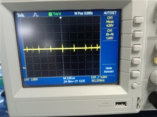
     output across C9 positive terminal and common ground.

  • Hello daniel, thanks for your reply.

    For the testing Vin cap we manage to mount capacitor in small loop and we found the noise is decrease a lot. Thank you so much for the support.

    Also i have update the layout please check below schematic and layout both, kindly verify 

    Please note red color net is GND.

  • HI

    the layout looks better than previous. but if you can turn diode 90deg C, let the Anode close to C8, it will reduce the parasitic inductance on this ground which will be helpful to eliminate the noise in the circuit

    and for ripple test, we more suggest you can test directly on the Capacitor instead of Common GND or at the input bypass cap of your load.