This thread has been locked.

If you have a related question, please click the "Ask a related question" button in the top right corner. The newly created question will be automatically linked to this question.

LP87524J-Q1: Stability problem

Part Number: LP87524J-Q1
Other Parts Discussed in Thread: IWR1843

Hi Team,

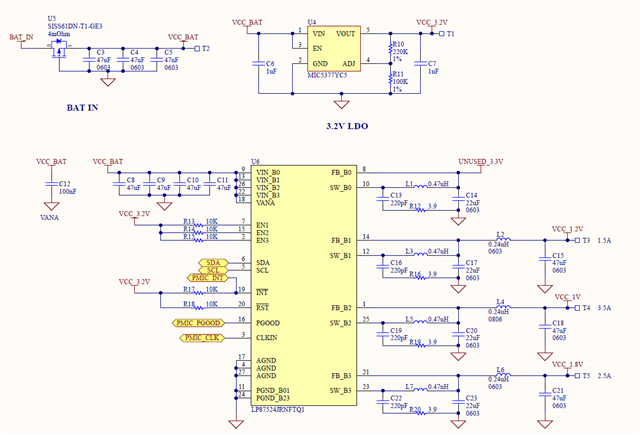
We use LP87524JRNFTQ1 for powering IWR1843 radar.

For last year we have a lot of power supply failures.

The most common reason is the failure of one or more LP87524 channels.

We observe the following symptoms:

1. During startup the switch works properly and output voltage increased OVER the predefined threshold.

2. After ~1 ms the switch stop working.

3. POWER_GOOD output settled to zero indicating failure.

Please see attached scope screenshot:

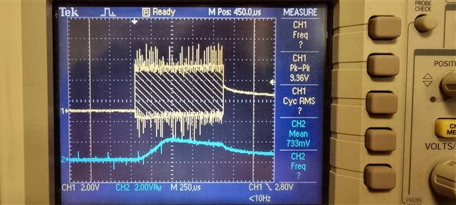
Here shown 1.2V channel. Channel 1 is a switch (pin12), channel 2 is feedback (pin14).

As you can see, the output voltage goes over 1.2V

A similar problem appears on other channels (1.0V 1.8V) on other boards.

When we replace the chip on PCB - sometimes it helps (the device started working normally),

sometimes not (or problem appeared in another channel).

We suspect the problem is caused by bad design and/or components (we use 0603 capacitors).

Could you please check our design and give us recommendations on how to solve the problem?

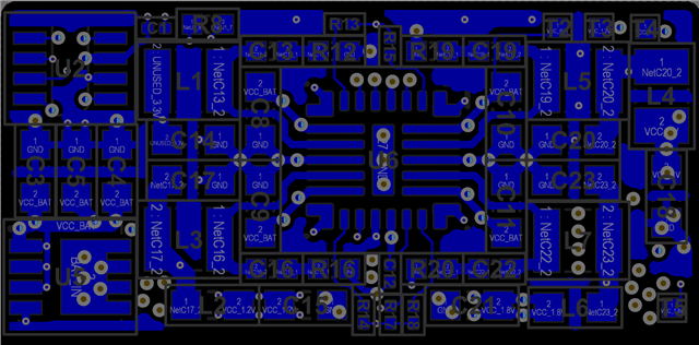
Please see our design:

Best regards,

Alex Ovchinnikov.

  • Hello Alex,

    Sorry to hear your troubles. Here's comments/questions about the design to help investigate the issue:

    - What is the supply voltage? Have you checked that it is stable/clean during startup and when bucks are loaded?

    - Capacitance right at the buck outputs can be quite low especially if 0603 caps are used. Recommendation is to have at least 2x22uF (nom) or 2x10uF (effective) at the output to make sure stability is good. You could try adding more output capacitance and see will it change the behavior. 

    - In the secondary LC filter the L looks quite high (240nH). We have used 100nH inductor (NLCV32T-R10M-EFRD). Performance was also verified with MPZ2012S101A ferrite bead and it could be used instead of 100-nH to save cost and space. Too high inductance can increase the output ringing during load transient. 

    - Have you tried to measure stability of the converters (phase/gain margin)? This would require cutting the FB line to be able to inject the measurement signal to the FB. 

    - How many layers are there in the board? The basic layout looks good, components are placed close to the PMIC and SW current loops are small

    - I could see one problematic connection in the layout. The C16 and R16 snubber is connected to the same GND via as the VANA supply bypass capacitor. So this effectively injects noise to the VANA supply, which should be kept away from the switching noise. All the references etc are run from the VANA supply, so it should be as stable/clean as possible. 

    - On the failing boards have you checked the FB pin(s) soldering to make sure the connection is strong? I'm just thinking what could cause the output voltage to rise above the target level. 

    Thanks.

    Regards,

    Tomi Koskela

  • Hi Tomi,

    Thanks for your quick responce.

    The supply voltage we use is 5V and it is stable during startup.

    The board has 8 layers. The PMIC is located on the bottom layer (L8),  L7 is a ground L5 is VCC_BATT.

    I tried adding additional capacitors but it didn't help. Perhaps the chip has already been damaged at this point.

    Is it possible that low capacitance combined with high LC filter inductance and wrong capacitor selection in the snubber network (we use 220pF/3.9Ohm) cause PMIC damage?

    We do not try to measure the stability of the converters (phase/gain margin) because it is very difficult to access FB. Do you have any recommendations on how to do it?

    Thank you to pointing out the problem with the possible VANA noise injection from snubber. We will fix it in the next PCB revision. Do you think this might cause the problems we had?

    I checked the FB connection on PCB and didn't see any problem. Moreover, the problem appeared on board that successfully works before...

    Another question - what is recommended connection for the exposed pad? We connect it to GND, is it ok?

    Thanks.

    Regards,

    Alex Ovchinikov.

  • Hello Alex,

    The snubber components are something you can also fine tune based on the PCB parasitics. The 390pF/3.9ohm were optimized for our EVM. You can check the SW pin overshoot/undershoot and try with different snubber components can you reduce the voltage spikes seen on SW pin. Measuring SW waveform with oscilloscope you need to be careful to keep the GND connection short (preferably with a spring type connection right at the probe tip, or using high speed differential probe) to get accurate results. For example SLVA255 document shows the principle of snubber optimization. Too high voltage spikes could potentially cause damage to the device. 

    Phase/gain margin measurement might be difficult if you don't have access to the FB traces. We usually recommend placing 0ohm resistors on the FB lines so that you could replace them with 50ohm (depends on the analyzer) for taking bode plots. Alternative way to check stability is checking the load step response and see how the output voltage settles. 

    Noisy VANA can cause all kinds of problems. You could check removing snubber components that connect to the VANA bypass cap GND does it have any effect. 

    Closer zoom to the output voltage/SW waveform during the overvoltage situation might help as well with the investigation. 

    Is the behavior on the 1.0V and 1.8V rails exactly the same? One major difference in the setup between 1.2V rail and the 1.0V/1.8V rails is that 1.2V rail has the PFM mode enabled. In PFM mode the buck cannot sink current and if there is leakage from somewhere else to the 1.2V rail the buck cannot regulate the voltage. In 1.0V and 1.8V rails bucks are forced to PWM mode and leakage from outside could not force the output high unless the leakage is in the 2A range or something like it..

    Center pad should be connected to GND. 

    Thanks.

    Regards,

    Tomi Koskela