This thread has been locked.

If you have a related question, please click the "Ask a related question" button in the top right corner. The newly created question will be automatically linked to this question.

BQ24715: bq24715 + CSD17308: Sudden death of the HS-FET

Part Number: BQ24715
Other Parts Discussed in Thread: CSD19537Q3, CSD18543Q3A, CSD17308Q3

Hello,

we are using the bq24715 as the main power controller of a battery buffered device. The battery uses two LiIon cells, so the system voltage is at 8.4 volts. Input voltage is 24 volts, and the circuit is pretty much the same as described in the data sheet and the EVM manual:

8738.bq24715 Circuit.pdf

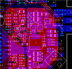
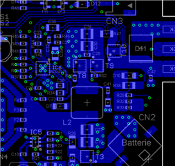
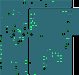
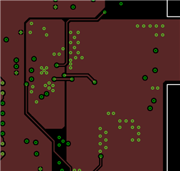
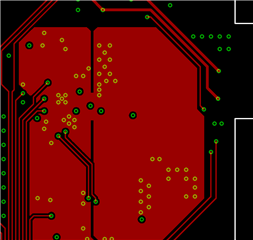
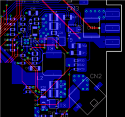
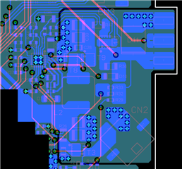
The PCB is a four layer board with this layout (outer layers only resp. all layers):

From a pilot series of 100 units, many (about 20) have already failed with a defect HS-FET in the switching regulator. We don't have any clue about what might have triggered the fails. Some units ran perfactly fine for days or weeks, and then suddenly failed. Others failed shortly after power-on.

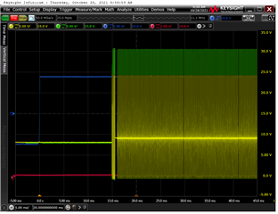
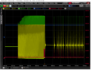
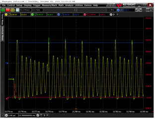
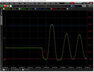
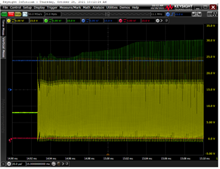
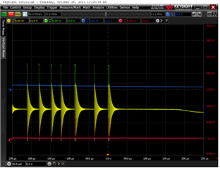
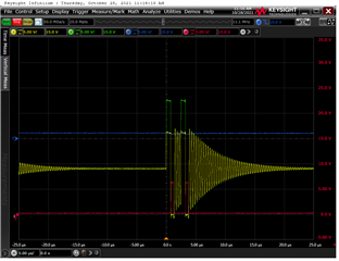
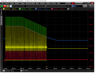
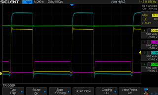
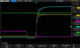
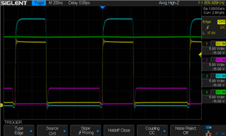
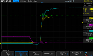
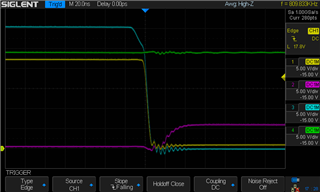
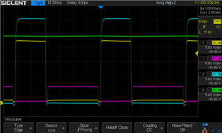
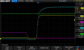
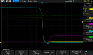
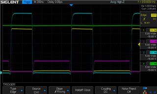
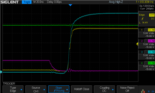
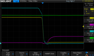
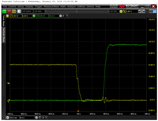
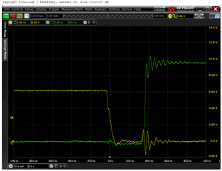
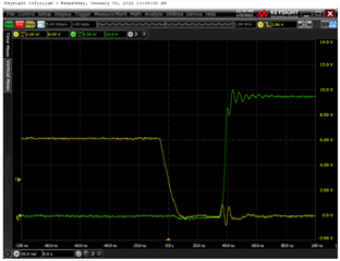
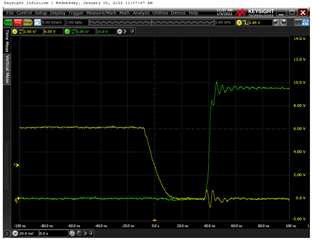
Everything that we have checked so far seems perfectly fine. Plug-in and plug-off of the 24 V supply results in perfectly correct behaviour of the regulator, and there also is no unusual thermal situation (at full load and under real working conditions within the enclosure, we measured HS-FET temperatures of about 60-70°C). Also, the switching signals appear perfectly fine with sufficient dead time:

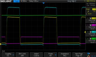
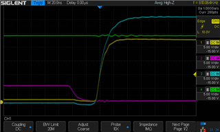
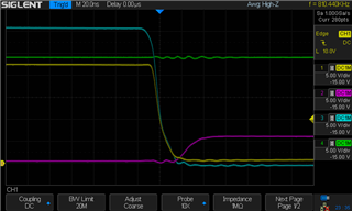
(Signal colors are obvious, however: yellow = PHASE, pink = LS gate, blue = HS gate, green = 24V input).

We would be very glad if someone had any idea what to look for... (We don't even know if this issue should be filed under bq24715 or CSD17308...)

Thanks & regards, Tilmann

  • Addendum: The failed HS-FET always show a D-S short circuit.

  • Dear Tilmann,

    What happens when you replace the defect HS-FET? Does the charge controller work again?

    Thanks,

    Mike Emanuel

  • In most of the cases, only the HS-FET is defect. After replacement, the devices work correctly again.

    However, at some of the devices the AC-FET also got a defect (like a strong G-DS leakage), and we also had a few defect bq24715 chips. We assume that these are subsequent fails, caused by the already shorted HS-FET.

    Regards, Tilmann

  • Dear Tilmann,

    We need to try to isolate the cause of the defects. Can you run a full charge cycle of the battery, recording battery voltage, battery current, and system current? I want to see if there is a particular battery voltage that causes the observed defect. Can you run this for several different boards?

    Thanks,

    Mike Emanuel

  • Dear Tilmann,

    It may be helpful as well to capture the input voltage. So in total, capturing the battery voltage, battery current, system current, and input voltage.

    Thanks,

    Mike Emanuel

  • Dear Emanuel,

    thanks for your suggestions. We have taken some measures, however to speed things up we did not run real battery charge cycles - instead, we simulated the battery with a two quadrant power source and so were able to check the systems behaviour at any battery voltage. Unfortunately, in this case, we did not get one single fail during many tests with several boards.

    And as the input voltage comes from a regulated power supply, capturing it would result in always the same value: 24.0 volts...

    However, today we experienced a fail in a completely different situation. We were bringing up and initializing a brand new board. For that, we applied the input voltage (24 V), but no battery or any other load was connected at that time. We programmed our bootloader into the microcontroller by SWD, and after that flashed the application, using that bootloader. When the application started after completion of the flash process, the HS-FET died. There was no load (except for very few mA taken by the micro), and the complete unit was cold. So load current, as well as temperature, could not have been an issue in this situation.

    When the application starts, it initializes the bq24715's registers with the settings we need in this application. Here's the sequence:

    1. Register 0x12 = 0x8544 (WD disabled, min.freq. 40 kHz).

    2. Register 0x14 = 0 (charge current off).

    3. Register 0x15 = 0x20D0 (max. charge voltage 8.4 V).

    4. Register 0x3F = 0x0500 (input current 1.28 A).

    After that, when the application is running, we regularly check the battery voltage and change the charging current according to it:

    - Above 8.2 V, 0x14 = 0 (charge off); re-enable at 7.9 V with 0x14 = 0x0200 (512 mA).

    - Below 5.7 V, 0x14 = 0x0080 (reduced charge at 128 mA), re-enable at 6.0 V with 0x14 = 0x0200 (512 mA).

    Sending register writes to the bq24715 is done only at the transitions, not constantly.

    In the case we just experienced, the charge current setting should have been unchanged at zero, since without battery we get a system voltage of first 9.0 V (bq24715 default), then 8.4 V (after init) - which is pretty safe above 8.2 V so the application won't change the setting again.

    Of course, we did not log the I2C communication at that very moment - maybe we should do that next week, when we try to reproduce the fail that way...

    Do you think that it might be caused by the init sequence anyhow?

    Thanks & regards, Tilmann

  • Dear Tilmann,

    I will get back to you by end of day Thursday.

    Thanks,

    Mike Emanuel

  • Dear Tilmann,

    What is your Minimum System Voltage (Reg 0x3E)?

    I saw no issues with that startup sequence on my EVM. I do not think it is related to the init sequence

    Thanks,

    Mike Emanuel

  • Dear Mike (please excuse me for calling you Emanuel),

    we do not change the value of the Minimum System Voltage register at 0x3E, so it should (still) be 6.144 V.

    I am not really surprised that you did not see any issues with the EVM. Take care that the fail shows rarely, and we don't have any clue about the trigger(s) yet. We have many boards running for weeks, partly months, without any problem. But then, all of a sudden, one might fail for whatever reason. Your single EVM with a limited test time does not provide statistically useful information...

    However, the latest fail here in our lab, with no battery and no load, is an evidence that it's not a thermal issue, and most probably also not an overcurrent issue.

    Is it possible that there is some kind of "weak point" concerning I2C communication? Maybe depending on the processes internal to the bq24715, if you access some register at a very particular ("weak") moment, could there be any unwanted side effects?

    Best regards, Tilmann

  • Dear Tilmann,

    Can you try increasing your pull-up resistors for the SMBus to the required 10 kOhm? The specification for SMBus specifies a maximum sink current of 350 uA and minimum sink current of 100 uA. Currently your sink current is 846 uA.

    Thanks,

    Mike Emanuel

    Please click "Resolved" if this answered your question.

  • Dear Mike,

    the 350 uA specification is explicitly related to the optional 1.1 kOhm series resistors to SDA, so that the required low level voltage still is met with these. It is not a general specification for SMBus. In fact, the bq24715 is specified with a load current of 5 mA (!) and still an output voltage of max. 500 mV which is a very safe "low". So, our pullup current of less than 1 mA is extremely well within the specifications.

    Additionally, I don't think that this can be related to HSFET faults in any way. Since we are only writing to the registers, the only time when the chip needs to drive SDA is the ack bit - and take care that it's open drain, so even a (theoretical) overload would only lead to an increased low level voltage, but never to destroying an external transistor at the power stage of the regulator...

    Best regards, Tilmann

  • Dear Tilmann,

    Can you capture the plug in event? Please capture the input voltage, VCC, PHASE, and input current. I want to see the plug in event to assist in the debug.

    Thanks,

    Mike Emanuel

  • Dear Mike,

    I am attaching a few screenshots from the bq24715 signals at power-up and power-down.

    1 (yellow) = PHASE,  2 (green) = HIDRV,  3 (blue) = VCC,  4 (pink) = LODRV.

    We didn't capture the input current at those measurements - but I doubt that would be of any help, due to the input capacitors.

    Also take care that it is not reproducible to cause a fail at power-up. We did very many power cycles without a single fail, as well as our customer. And there are reported fails that happened suddenly at normal operation without any external triggering event. The only thing we can tell after the single power-on fail we experienced here: it does not necessarily require a battery, a system load or a higher temperature for the fail to occur.

    Regards, Tilmann

  • Dear Tilmann,

    Can you please confirm the failure of the HSFET (ie if its shorted etc.)?

    The very first waveforms you sent me had the bandwidth limit of 20 MHz on. Can you please recapture those images but with no bandwidth limit? Please use as small as possible of a loop between the ground lead and probe, using the tip and barrel method if you are able.

    Thanks,

    Mike Emanuel

  • Dear Mike,

    yes, the fail is always a D-S short (please see the addendum in my first "reply" to myself, after I noticed that I forgot to mention that in the OP - and you already responded to that one).

    The BW limit was a mistake, we'll take new screenshots.

    Regards, Tilmann

  • Dear Tilmann,

    Got it! Looking forward to your captures!

    Thanks,

    Mike Emanuel

  • Dear Mike,

    here we are:

    Regards, Tilmann

  • Dear Tilmann,

    There is some ringing on the gate drive waveforms. Can you please insert a 5 or 10 Ohm gate resistor in series with LODRV and HIDRV to see if this causes any improvement?

    Thanks,

    Mike Emanuel

    Please click "Resolved" if this answered your question.

  • Dear Mike,

    here are some measurements with 5 ohm gate resistors added:

    Also, there is a new layout revision "R2" with improvements in EMC behaviour, particularly regarding radiated emissions. We changed from one ground plane to three, and also improved the GND connection of the bq24715. Here are the R2 screenshots, first without gate resistors:

    And R2 with additional 5 ohm gate resistors:

    Do you really think this could explain the sudden deaths of the HSFETs?

    (Before we could gain any statistically valid information, we'd need to patch all those 100 devices that are currently under test. This is quite some effort, and also will take some time...)

    Regards, Tilmann

  • Dear Tilmann,

    These look better! Before you modify any more, can you show the results for a 10 ohm gate resistor so I can compare as well? I think it is something worth looking into!

    Thanks,

    Mike Emanuel

  • Dear Mike,

    while I agree that these "look better", there are some questions:

    - Do you really think that this ringing could ever cause a sudden death of the HS-FET? Sometimes at power-up, sometimes after hours, days or even weeks of perfectly fine operation? And without any thermal abnormalities? What would be the exact failure mechanism? (Just "looking worse" does not explain fails...)

    - What about the revised "R2" PCB layout, which without additional gate resistors has similar waveforms like "R1" with them? Would it make sense to add these gate resistors there as well? (R2 will be the future series production release.)

    Of course we can try with 10 ohms gate resistors as well, however not today... And note that adding gate resistors also has limitations: when we tried to improve radiated emissions by adding gate resistors, we found that the circuit does not work any more as soon as we increase them beyond 10 ohms. So that would be pretty close to the operational limit, which is not a good basis for series production...

    Regards, Tilmann

  • Dear Tilmann,

    In the original waveforms you sent me, the LODRV oscillates to over 2 V after it turns off. The threshold voltage of the chosen FETs is 0.9 V minimum. This oscillation can potentially can cause shoot through of the switching FETs. This phenomenon needs to be managed as shoot through can permanently damage the FETs. 

    Also, it appears as if there is some ringing in either case when the LSFET is off. I am wondering if this is related to your GND connections. As I review your layout, I see you only connect Pin 14 to GND at the C26 connection through one via. I would highly recommend connecting the physical pin 14 to the Power Pad directly. This is shown in the BQ24715 EVM User Guide. In addition, more vias from near the GND pin to the GND layer will reduce via inductance. 

    Thanks,

    Mike Emanuel

    Please click "Resolved" if this answered your question.

  • Dear Mike,

    thanks for your explanation.

    The "R2" layout is improved particularly with respect to the GND connections of the bq24715. Before, we were trapped by the faulty data sheet and EVM manual which explicitly tell us to NOT connect the GND pin to the exposed pad... You can see the previous discussion here: bq24715-high-inacceptable-radiated-emi-emissions-under-load

    So, after that layout revision, it appears interesting that the ringing of the R2 version is not too much better than that of R1. Even with the gate resistors, the amplitude of the LSFET gate ringing is not significantly lower. And if we add more gate resistance, we'll run into even more problems due to the weaker drive and the LSFET being turned on by its miller capacitance...

    It's evening here, and I don't have the design files at hand now. I will provide some layout information of the R2 revision tomorrow. And surely we will need to look closer at those signals...

    Thanks, Tilmann

  • Dear Tilmann,

    Looking forward to hearing back from you!

    Thanks,

    Mike Emanuel

  • Dear Mike,

    here are some views of the system supply part of the new R2 board layout (outer layers first, then all four layers separately):

    You can see that the main changes are the GND connection(s) of the bq24715 and the use of now three layers as ground planes. We also added optional gate resistors and an optional snubber at PHASE.

    I took some screenshots with a faster scope. These were taken with the R2 layout, and with already assembled gate resistors of 5 ohms each.

    LODRV at turn-off:

    And PHASE at turn-on:

    One can still see that there is a small disturbance at the rising edge of PHASE, probably because the LSFET is becoming conducting again...

    This might as well be a result of the rising edge at PHASE and the miller capacitance of the LSFET. It's interesting that the LODRV signal is perfectly smooth first, but then suddenly there is some intensive ringing... So using gate resistors might even be the wrong direction?

    And what could we do against that? With the current layout, do you see any detail which we could improve?

    Regards, Tilmann

  • Dear Mike,

    two more screenshots... This is LODRV of the EVM at the same load:

    And this is LODRV of our R2 board, but now without gate resistor at the LSFET (I kept the resistor at HIDRV to not increase the HS turn-on speed):

    That's better than with the 5 ohms in series, but still slightly worse than the EVM.

    Regards, Tilmann

  • Dear Tilmann,

    I am starting my Christmas break and will not be able to answer regularly.

    Some suggestions for the GND pours:

    1. In the EVM layout, the REGN GND is tied to the same GND as the input capacitor GND. It looks like you are partitioning the REGN GND to be with the GND pin. Please follow the EVM layout.

    2. I would recommend against having the island of GND pour you have in the brown layer. You can separate the analog GND and power GND without creating an island. Please refer to the EVM layout.

    Thanks,

    Mike Emanuel

  • Dear Mike,

    I am getting slightly frustrated by the contradictory informations we get... In the other thread, I exactly asked the question to which ground the REGN capacitor (C26) should be connected. Argh... The documentation should be much more precise (and correct, at first...) in this concern. As a developer, I really need to know which pin carries which current.

    It's also not possible to follow the EVM layout exactly here, since that populates a few parts at the bottom side of the PCB, which we can't do here. And since the pads are much closer to each other than the discretes can be placed, some of them need longer traces or end up somewhere else... In the EVM, the GND connection of the REGN capacitor is located right at the bridge between the grounds, however this is impossible here.

    Additionally, the REGN voltage is used primarily when the LSFET is turned ON - however the "miller problem" we have is at the moment after the LSFET has been turned OFF. At that very moment, all the gate driver needs to do is keep the LODRV at ground level - as hard as it can. For that, the gate current needs to flow out of GND and/or EP (wherever it really is connected to, internally...) with minimum stray inductance. This is apparently achieved with our current layout.

    The "island" in layer 3 is just because connecting PGND and AGND with two of the three ground layers should be sufficient (see the bridges in layer 2 and 4). In fact, layer 3 would add only marginal copper here, unless we'd make the bridge between the two grounds significantly wider.

    However, even the EVM shows almost the same amount of ringing at LODRV. So maybe that can't be improved too much further anyway?

    Thanks & regards, Tilmann - and merry Christmas!

  • Dear Mike,

    when looking more closely, I just noticed that the EVM adds another 470 pF (C24) to LODRV, effectively almost doubling the input capacitance of the LSFET. Well, this will of course reduce the voltage spikes induced by Mr. Miller at the rising edge of PHASE. This capacitor is not mentioned anywhere in the data sheet, and since some other parts of the EVM are optional and not assembled, I overlooked that before.

    We might try adding a small cap at LODRV as well. And eventually look for alternative LSFET types with smaller D-G capacitance - what do you think?

    Regards, Tilmann

  • Dear Tilmann,

    I am sorry you are frustrated. This process is iterative and will take some time to resolve.

    I would recommend trying to add a small capacitor at LODRV (like in the EVM) to see what improvements can be made. Smaller D-G capacitance and higher threshold voltages would both be things to look at for alternative LSFETs.

    Thanks,

    Mike Emanuel

    Please click "Resolved" if this answered your question.

  • Dear Mike,

    I am not frustrated by the fact that iterations are needed to solve this problem. What puzzles me is the inconsistent and partly contradictory or just plain wrong information provided in the available documents. The precison and correctness of information in these documents should really be improved. That would have avoided many of those iteration steps as well...

    Besides, many thanks for your help, which I really appreciate.

    When looking for alternative LS FETs, can you provide any suggestion(s)? I already searched some time, but without really promising results...

    Thanks, best regards - and all the best wishes for 2022!

    Tilmann

  • Dear Tilmann,

    I would tend to focus more on finding something with a slightly higher minimum and typical threshold voltage, as the provided D-G capacitance is already fairly low. Try to match or increase the VDS rating of the original FET if possible, and make sure the RDSon is comparable. Please select an appropriate current rating as well. I would try to match the HS and LS FET if possible.

    How did adding the capacitor at LODRV help?

    Thanks,

    Mike Emanuel

    Please click "Resolved" if this answered your question.

  • Dear Mike,

    yes, that are the criteria. However, as mentioned before, I have already been searching quite some time for FETs that might be "better" in this situation - without finding any. Perhaps you can get more concrete and provide part numbers to look at?

    Since this is the 2nd working day after Christmas/New Year, we did not yet take measurements with the additional gate capacitor. Also, I'd rather work against the cause of the problem instead of fighting symptoms... A "better" FET with be the better solution, and also avoid additional load for the (apparently too weak) LS gate driver within the bq24715.

    So, please, which other FET could be considered as "better" here? (With a higher threshold, but still low RDSon at 5 V; with perhaps lower capacitances, but still VDS >= 30 V; with a package in the same size range and thermally equivalent; ...)

    Thanks & regards,

    Tilmann

  • Dear Tilmann,

    I would like to see the benefit of adding the gate capacitor as this can potentially avoid new part selection.

    Here are several examples I found. I cannot guarantee the performance as this is a charge controller and I have not tested these combinations myself. Also, please note I was not always able to get the same package.

    1. CSD19537Q3: Minimum 2.6 V gate threshold, 1290 pF input capacitance, 13.3 pF reverse transfer capacitance, 13.8 mOhm at VGS = 6 V.

    2. Si7288DP: Minimum 1.2 V gate threshold, 565 pF input capacitance, 42 pF reverse transfer capacitance, 18.0 mOhm at VGS = 4.5 V.

    3. SiR426DP: Minimum 1.2 V gate threshold, 1160 pF input capacitance, 70 pF reverse transfer capacitance, 10.4 mOhm at VGS = 4.5 V.

    Thanks,

    Mike Emanuel

    Please click "Resolved" if this answered your question.

  • Dear Mike,

    many thanks for the parts suggestions. Before, I rather looked at the 30 and 40 V devices, since those for higher voltages normally had much higher resistance, higher capacitances, or both...

    But now, when searching more deeply, I found an alternative type that appears to be even far better than the CSD19537Q3 which you mentioned.

    CSD18543Q3A: Min. threshold 1.5 V, 885 pF input, only 4.8 pF (!) reverse transfer capacitance, 15.6 mOhm at 4.5 V.

    This makes for a "reverse capacitance ratio" of only 0.54%, while the CSD19537Q3 has 1.03% and the currently used CSD17308Q3 has 5%... (The Si types above are even beyond that ratio...)

    I would REALLY like to test this device - unfortunately it is made of pure unobtainium. Do you see any chance that we can get several samples of this one? Earlier, I was able to request samples directly from the TI website when being logged in, however this service seems to have been disabled for our account for whatever obscure reasons...

    Here are some more screenshots:

    a) Layout revision R2 (the current, optimized layout), without and with 470 pF at LODRV

    b) Layout revision R1 (bq24715 GND separated following the data sheet), without cap and with 470 pF or 1 nF

    It can be seen that the additional capacity of 470 pF (as expected) roughly halves the voltage pulses at LODRV that are caused by Mr. Miller. The newer R2 layout appears to be rather uncritical even without additional capacitor. Interestingly, adding an even larger capacitor (1 nF) at the R1 layout does not result in a significant improvement at this point, so adding 470 pF there seems to be a reasonable patch to the existing boards to at least reduce the failure risk.

    Any help in getting CSD18543Q3A samples is greatly appreciated.

    Thanks and best regards,

    Tilmann

  • Dear Tilmann,

    It certainly looks like the 470 pF improved layout revision R2. What is the peak of the ringing? What happens if you test this for long periods of time on other layout revision R2?

    I can see the 470 pF and 1 nF capacitor improve layout revision R1, however there is still some ringing on the green waveform.

    The best way to get ahold of samples would be to click the "Contact TI" hyperlink on the product page which sends you to the "Customer Support Center."

    Thanks,

    Mike Emanuel

    Please click "Resolved" if this answered your question.

  • Dear Mike,

    you can estimate the peak amplitudes from the scale at the right side. Even without the additional capacitor, the ringing is safely below 1 V for the R2 layout revision - that's why I noted this as "rather uncritical". We might add the cap in series production, though...

    The ringing on PHASE (green) of the R1 revision might also be influenced by the generally higher ground impedance (in R2, we use three solid GND pours, while R1 only has one) and the position where the probes GND tip was located.

    We REALLY would like to take measurements with the CSD18543, however even the Customer Support Center was not able to help. No stock at all, no information about lead times...

    We'll surely stick to the additional gate capacitors for the time being, and postpone the CSD18543 tests until better times.

    Many thanks for all of your help - and best regards,

    Tilmann