This thread has been locked.

If you have a related question, please click the "Ask a related question" button in the top right corner. The newly created question will be automatically linked to this question.

LM5102: HO/LO state when VDD is 0~9V

Part Number: LM5102
Other Parts Discussed in Thread: LM5106, TINA-TI, LM5109B

Hi Team,

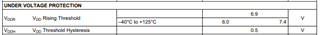
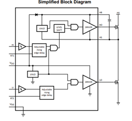
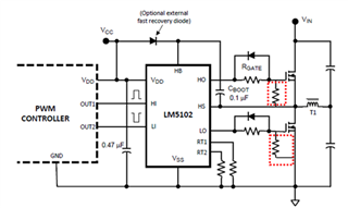
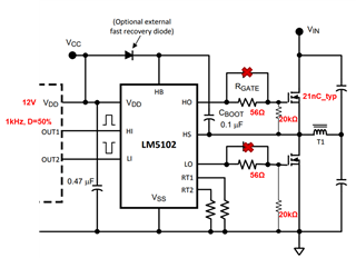
I have a simple question about LM5102 HO/LO state when VDD is 0V and 0~9V(below recommended operating conditions).

Hi-Z, pull up, pull down?

I think 0~9V is unknown state though.

Regards,

Kai

  • Hello Nomiyama-san,

    The driver has a feature called UVLO, shown in this table.

    This works in the driver like this:

    See the UVLO block that feeds into the AND gate?  The AND gate being low means that the driver will be in a pull-down state. UVLO also has a hysteresis so the exact thresholds vary depending on if you are rising or falling on VDD. Assuming everything is typical, for falling, from 9 to 6.4V (6.9V - 0.5V hysteresis) the driver should continue to operate. Pullup or pulldown  will be determined by the input. Below this, the driver will be pulldown no matter the input. However, once VDD gets low enough (the exact threshold is not measured), the bias is not enough for the IC and the blocks stop functioning correctly. This would result in a somewhat HI-Z/unknown state on the outputs, but because of ESD diodes and body diodes, it likely won't be very high impedance. Hopefully this was helpful.

    thanks,

    Alex M.

  • Thanks Alex,

    In order to make sure output pull-down during "VDD gets low enough", when we put pull-down resistor to HO/LO, do you have any recommended value or any selection guide?

    Here is requirement for LM5102.

    VDD: 12V

    VIN: 30V

    RT1/2: 100kohm

    Rgate: 56ohm (no gate diode)

    input: 1kHz

    PD: put pull down resistor like below.

    Regards,
    Kai

  • Hello Kai,

    Anywhere between 10-20kohm is usually a safe choice for this purpose. The current draw will be roughly VDD/Rpulldown so with 10k you will have about 1.2mA draw when ON and with 20k it would be 0.6mA. However, with such a low frequency of operation, you should be careful with the Bootstrap voltage. Here are some quick calculations:

    I = C * dV/dt & I = VDD(12V) / Rpd

    12/Rpd = Cboot * (ΔV / Ton(500us)) 

    ΔV = 0.006/(Pd*Cboot)

    The reason I bring this up, is because a 10k pulldown and 100nF bootstrap capacitor will mean roughly a 6V drop on HO as you run. Here is a simulation showing this:

    What bootstrap capacitance are you using? A larger capacitance should help reduce this problem, especially since you are operating at such a low frequency. If you want to simulate this, you can use the LM5106 model. They have extremely similar functionality.

    To summarize, a Vgs pulldown is fine, but just be sure it doesn't cause problems for your high-side bootstrap circuit.

    thanks,

    Alex M.

  • Hi Alex,

    I summarized each parameter in attached excel file for customer requirement.
    Calculated Cboot value is 5nF and customer uses 1uF as Cboot.

    I tried to simulate with LM5106 model but I couldn't simulate it due to error.
    I use attached TINA-TI to estimate 20kohm PD. HB minimum voltage looks 8.65V(9Vmin-350mV※diode Vf=750mV so add 350mV since VDH=1.1Vmax) > 6.7V(VHBR-VHBH) but could you double check below configuration works well?


    In addition, datasheet mentions below but figure 16 VDD bypass capacitor is 0.47uF which is not 10 times greeter than 0.1uF CBoot.
    Is it typo or what Vdd bypass capacitor value should be used in this requirement?
    "As a general rule the local VDD bypass capacitor should be 10 times greater than the value of CBOOT."

    LM5102_Boot_Strap.TSC

    LM5102.xlsx

    Regards,
    Kai

  • Hello Kai,

    The configuration looks good. Are you planning to use the external boot diode in the design? It may not be necessary. I also have had issues with the LM5106 model, but using the LM5109B model (which is moderately close), I was able to simulate this and it was close to my predictions. due to the pulldown, you will likely see about 0.5V drop on HO over a cycle, which isn't much of a drop. With a large bootstrap, it may take a few cycles for the bootstrap capacitor to charge up to VCC-Vfd, but once it reaches steady state it should be okay. 

    The VDD bypass capacitor being >10x Cboot is just a suggestion to keep VDD from dropping too much when Cboot is charging. This diagram was likely made before we adopted that suggestion, and was never updated. I would recommend following the 10X Cboot suggestion, but make sure the VDD bypass is larger than the Cboot at the very least. Also, we tend to recommend adding a smaller VDD bypass cap (100nF or so) in parallel to better filter out high-frequency noise. 

    thanks,

    Alex M.