This thread has been locked.

If you have a related question, please click the "Ask a related question" button in the top right corner. The newly created question will be automatically linked to this question.

TPS63000: L2 and GND pins are getting shorted randomly.

Part Number: TPS63000

Hi,

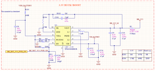
We have a few design where we are using "  TPS63000IDRCRQ1" , " TPS63000" and  "TPS630001" since last 2-3 years but we are facing consistent issue.

For the Developmental testing purpose when we try to change o/p capacitor or try to tune feedback resistor divider values, we notice that sometimes above Ics start consuming high current 30mA to 150mA at no load.

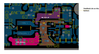
When we debug circuit we get to know every time L2 pin is getting shorted with  GND pin.

Please note that we are facing same issue in multiple design not in single design.

Please help us to understand where can we get wrong.

If possible please provide a workaround or solution for it.

  • Hi  Jyoti,

    i think your description about "try to change O/P capacitor" means try to decrease the ouput cap and "try to tune feedback resistor divider values" means try to increase the output voltage by change the resistor divider, right?

    if it is ture, i am afraid  peak voltage of Pin L2 is out of spec, and FET internal is damanged.this spike is not only has relationship with the output voltage but also the parastic inductor. 

    try to improve, you can decrease the parastic inductor by good layout(you can take user guider as ref)  and please do not remove the output cap which is close to device.

    Regards

    Tao

  • Hi Tao Zhang,

    Thanks for the response.

    Let me explain my use case.

    We had BB (TPS63000, adjust.) configured with 3.3V o/p. with two 10uF Capacitor at o/p in original design.

    Later we decided to switch to 2.8V o/p and  increase o/p capacitor value to 47uF and 47 uF.

    Procedure we follow:

    1. remove all power sources to device.

    2. Use soldering iron to remove old o/p cap and assemble new o/p cap.

    3. use solder to remove resistor (of voltage divider at feedback) and put new value resistor.

    4. We make sure no solder flow to any other pin  or component.

    5. we always clean our PCB before powering up.

    6. then we power up our device to do further test.

    note: we use 2X AA primary battery (3V).

    Issue:

    when we power up our device and start measuring voltage and current. several times it happens that our device start take current in mA even at no load.

    when we check IC pin -2 (L2) shows shorted with GND.

    Then we replace TP63000 with new one and device start working fine.

    I doubt if it is ESD issue that we might  happen during soldering??

    Note: we we antistatic Lab setup to do any assembly.


    I am attaching schematic and layout file for your reference.

    I think inductor placement is fine in layout. (8 layer board,)

  • Hi  Jyoti,

    seems all my suspect go wrong. Joy

    ESD issue seems very possible, but i am not sure and it is hard to confirm, right?

    another point is, with larger output cap, you will get a higher peak current or same peak current but lasts for a longer time during start-up. then  it will cause a higher spike in node L2 or same spike but lasts longer.i think you can check it by capture waveform during start-up and make sure spike is not out of spec.

    Regards

    Tao