This thread has been locked.

If you have a related question, please click the "Ask a related question" button in the top right corner. The newly created question will be automatically linked to this question.

UCC5310: Using negative bias but still have self turnon

Part Number: UCC5310

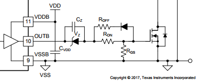
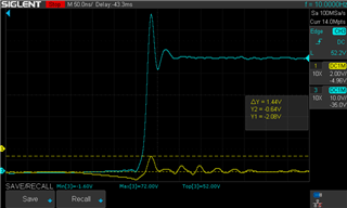
I'm having an issue where I'm implementing a negative turn off bias as described in this thread. Unfortunately I'm still somehow experiencing self turnon events despite the induced gate voltage spike being in the negative voltage region and supposedly well below the threshold voltage of the mosfets being used (VGS(th)min = 3.0V).

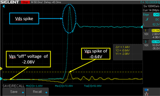
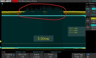
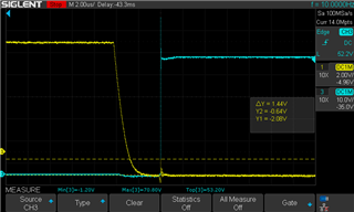
I try to focus on the turnon event(s) in the included images. Measurements were taken right where the mosfet legs enter the TO package and low-inductance measurement techniques were used with ground springs and short connections. These particular measurements are of the low-side mosfet of one of the 3 phases. The high side mosfets display similar but less severe behavior. Chanel 1 is the Gate votlage (Vgs). Chanel 3 is the switch node (Vds).


The miller clamp of the UCC5310MC device has been removed from play else it would discharge the negative bias built up by the 10uF capacitors. The clamp alone was not enough to stop the turnon events either and I've already increase the Cgs capacitor to a relatively high value. 

Any ideas on what might be going on here?

  • Hi, Lucas,

    Nice to hear from you again!

    I suspect the issue is it doesn't appear you've implemented your split supply as shown in Figure 61 of the datasheet. You need to keep the gate drive loop from OUT to VEE2 as short as possible to minimize the parasitic inductance there. In Figure 61, it's for a different version of the IC which has a GND2 terminal, in your case, since you're using the UCC5310M, that node will be a "virtual" node.

    And, as Derek noted, the diode/capacitor combination isn't something we commonly see done with our gate drivers. You may try replacing the 10 uF cap with a resistor to see if that helps the situation. You could also try connecting the CLAMP to your GateHC and GateLC nodes. I don't see where those are connected to anything; are those just test points?

    Best regards,

    Don

  • Hey Don! Thanks helping here.

    I haven't implemented split supply. I am creating a negative bias like from the example below and from thread I referred to. Even though it's not split supply, it is creating a negative bias for negative turnoff voltage. VEE2 is still connected to the source of the mosfet through a large plane. Would there still be an issue here with a virtual node in the device being referenced differently than VEE2 and somehow rendering the negative bias ineffective? 


    The 10uF Cz cap is working with the zener diode to generate the negative bias. It is required for this approach and the value must far exceed the total value of GS capacitance. Replacing this cap with a resistor would defeat this approach to creating a negative bias. 

    The clamp used to be connected to GateHC and GateLC but I removed it from play as stated in my original post. It was not strong enough to suppress self turn on and having it in play actually keeps the negative bias from building up. 

    All things considered, I'm still unsure why the negative bias isn't helping. 

  • Hey, Lucas,

    Can you label the oscilloscope plots above with where they were taken on your scope plots for me?

    Best regards,

    Don

  • Hello Lucas,

    I see you have been working with Don on this issue. Don must be out of the office at the moment and should be able to address your questions within the next day.

    Regards,

  • Hey guys it's fine. We can also take this to email if it helps. Below is the requested labelled scope shot.


    These were taken right at the MOSFET legs were they meet the TO-247 package body. So Channel 3 (Blue) is taken across drain and source(Vds). Channel 1 (yellow) is taken across gate and source (Vgs).

  • I may have misdiagnosed the issue here. It may not be a self turnon issue at all and actually be a reverse recovery issue. Hence why even pulling the gate voltage in the negative region for the off state did nothing. I'm gunna slow the high side mosfet turn on time and see if it helps. If this is actually the case, do you guys have any recommendations on how to improve this? 

  • Hi, Lucas,

    Yeah, your gate to source measurement is way too low to get any turn-on. You do have a pretty large spike on the VDS. This may be due to parasitics on the board causing that large spike, especially the loop of decoupling from positive rail to ground.

    Let me know what you find out in further analysis. What is the actual behavior you are seeing that is concerning you?

    Best regards,

    Don

  • Don,

    I think I've got it. Its a combination of the adjusting the ON slew rate of the gates and dead time. For testing, I had inserted a large amount of dead time to prevent shoot through during initial evaluation. However, I didn't know that this excessive deadtime increases the reverse recovery current flow. So a combination of too fast of ON time and too long of deadtime was leading to the spikes. Reducing dead time down to the minimum amount actually needed and slowing down the ON time has helped so far in low power/current testing. I'm marking as resolved for now and I'll provide any further updates should they be meaningful.