This thread has been locked.

If you have a related question, please click the "Ask a related question" button in the top right corner. The newly created question will be automatically linked to this question.

BQ25887: Enabling the ADC not possible

Part Number: BQ25887

Hello 

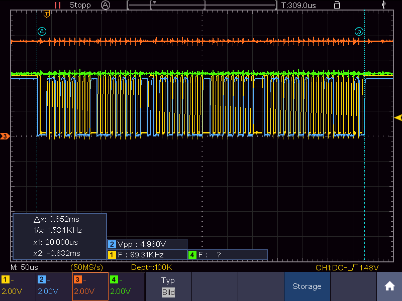
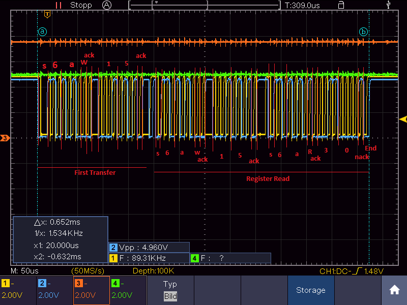
I am using the BQ25887 on the balancer 5 click board (PID: MIKROE-3853) and I have a question regarding the ADC control register (REG15 register). I read the subsection 8.3.5 (Integrated 16-Bit ADC for Monitoring) and I have tried to configure REG15 and enable the ADC with the ADC_EN bit. Afterwards I checked if setting the register was successful but found out that the reset value which is 0x30 is still there. I have already checked if the conditions

VVBAT > VBAT_UVLO_RISING or VBUS > VBUS_UVLO_RISING

are met and this is true for either setting. I have already checked the I2C signal and if the transmission is correct. Can you tell me what else I can check or what I might have overlooked since I can't manage to fix this problem.

Best regards,

Markus

  • Hi Markus,

    Given that the voltages are above the necessary thresholds, and the register value (0x30) implies continuous operation, it is possible that the bit is being reset through either the Watchdog timer or setting REG0x25 bit 7. Can you confirm the duration of your watchdog timer and the time between setting the bit and reading it back? Additionally, can you confirm that registers REG0x17 to REG0x27 have a value of 0x00 and provide the value of REG0x16.

    Lastly, can you please confirm the value of VBAT and VBUS in your application, and ensure with a waveform that these voltage are constant and not falling below any thresholds? 

    Best Regards,

    Juan Ospina

  • Hello Juan,

    Thank you for your answer. I have tried your suggestions.

    Bit 7 of REG0x25 is cleared (and not set by software).

    The duration of my watchdog timer is set to 40s (WATCHDOG[1:0] := 01).
    Setting the ADC CTRL register REG0x15 (enabling the ADC) and reading the content
    immediately afterwards takes 0.652ms (see image).

    The voltages VBUS := 5V (CH4) and VBAT1 := 7.9V (CH3) are above the required thresholds (VVBUS > 3.3V and VBAT > 4V).

    The ADC Function Disable Register (REG16) is set to 0x00 and all ADC read
    registers REG0x17 to REG0x27 have the value 0x00.

    Is this what you have suggested? Unfortunately the problem is still there.

    Best regards,

    Markus

  • Hi Markus,

    Based on voltage values, the ADC should be available for use.

    Based on the I2C transfer waveform, there appears to be 2 transfers however the first transfer is incomplete, and the second is a normal register read. If the first transfer is intended to be the register write that would enable the ADC, then this may be the reason that the adc is not enabling as intended. This is the intended structure of a write:

    But based on the waveform only the Slave Addr and Reg Addr is transferred:

    Does the write to REG0x15 occur at a different time than this waveform shows? If you attempt to execute the write and the read separately and manually, does this allow the adc to enable?

    Best Regards,

    Juan Ospina