This thread has been locked.

If you have a related question, please click the "Ask a related question" button in the top right corner. The newly created question will be automatically linked to this question.

LP87524J-Q1: Schematic review

Part Number: LP87524J-Q1

Hi Team,

There is a good new that we DIN  LP87524JRNFRQ1

And there have one thing need your support!
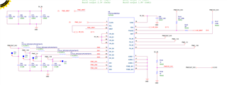
Please help check this SCH, THX

And customer feedback LP87524JRNFRQ1 is damage during RMA,!  Has a similar incident occurred in LP87524JRNFRQ1? THX

  • Hello Kygo,

    Please see the schematic/layout checklist to help with the design: https://www.ti.com/lit/zip/snvr480

    Comments about the schematic:

    - For 5V input voltage snubbers are needed on each SW pin. 

    - Check stability considerations for total output capacitance on each buck: https://www.ti.com/lit/an/snva881/snva881.pdf 2x22uF output capacitance on each rail is the minimum, but depending on input/output voltage more might be needed.

    - Is this a radar system? It would be good to check the secondary LC filters before the AR supply pins.

    What is RMA? These devices are robust as long as good layout is followed and other design rules for good stability (sufficient output capacitance), supply voltage is stable. Also snubbers in SW pins are important and must be used for 5V supply voltage use case. 

    Thanks.

    Regards,

    Tomi Koskela