This thread has been locked.

If you have a related question, please click the "Ask a related question" button in the top right corner. The newly created question will be automatically linked to this question.

BQ25792: BQ25792 Battery IC heated and burnt without connecting any battery

Part Number: BQ25792

Hi

I'm using below battery charging circuitry, please refer.

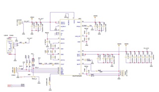
Here input is 12V and pin configuration is made for charging a battery which  is in 4S type. 12V_SYS was giving 12V which is supplied from 12V supply and this was powering other circuitry.

CS pin was connected to ground permanently. CS pin once shorted to ground, enabled LED to glow initially, but it stopped glowing after some time.

Here i'm expecting voltage at REGN pin to be at 4.8V but 0V is appearing. Initialing input current at power source was  set as 0.5A and the IC was getting heated. Since board was working properly to support additional load, we increased the current to 2A at input source. This resulted in exponential increase in heat generation and IC got burnt.

In all the above cases, battery was not connected and BATP pin was left floating. Thermister was connected initially but removed later since battery was not connected,

Please let me know whether something is wrong with this schematic. Do i need to

  • Hi Bivin,

    On the schematic, the only potential issue I see is too little capacitance on PMID.  With input power attached, REGN should be approx 5V.  If CS = /CE pin and with thermistor attached but no battery, the IC pulses in and out of BATOVP and SYSOVP.  If you increased input power and the IC was damaged and not protected by its redundant protection circuits, then it is possible that there is a PCB short.  This IC is also very sensitive to board layout.  If the PCB does not follow the board layout per the datasheet and the EVM user's guide (especially having the PMID and SYS 0.1uF capacitors as close as possible to the IC with no vias), it is possible that the OVP events damaged the IC. 

    Regards,

    Jeff 

  • Hi Jeff

    We are having an undamaged board where the IC is working. I2C is working and we are able to read device ID without connecting battery and by setting only 0.5A current.

    Also there is not short on the battery and related circuitry.

    As per datasheet, for charging battery in 4S (16.8V) configuration using 12V supply, "The source current rating needs to be at least 3A for the buck-boost converter of the charger to provide maximum output power to SYS.", we need to set source current as 3A.

    While doing the same, we will connect both battery and thermister and we will make /CS pin '0'. In the above case, is there any possibility of IC damage or the voltage overshoot at SYS  pin. How can we safely test the IC without damaging it.

    Please advice.

    Regards

    Bivin

  • Hi Bivin,

    As long as the PCB follows the recommended board layout, I am not aware of any ICs being damaged by operating at 4S.  Please send me your PCB layout information.  Also, can you send a scope shot of SYS, BAT and SW voltages at power up and when the OVP events occur (i.e. with thermistor attached but battery not attached).

    Regards,

    Jeff

  • Hi Jeff

    I connected thermistor without battery and CS pin connected to ground.

    After increasing current to 2A, board didn't powered ON, so immediately turned off supply. I found that PMID pins, SW pins , REGN pins are shorted to ground.

    Attached a detailed report on the same. Kindly go through.

    Battery IC-test.docx

    Also we found that after removing SW inductors, only SW1 is shorted to ground in addition to PMID & REGN pins. Caps at PMID & REGN pins were verified and they were not damaged.

    Please comment.

    Regards

    Bivin

  • Hi Bivin,

    From the layout it appears that the 0.1uF decoupling and bulk capacitors for PMID and SYS connect only through a very small (green) trace to the IC pins, with the bulk capacitor grounds connecting through vias.  Unfortunately, we found that that the PMID and SYS capacitors must connect to the IC pins on the same layer as the IC with no vias.  If not, unfiltered switching noise causes issues with the voltage regulation loops.  On our first revision of the EVM with a similar layout we saw IC damage like you are seeing.  By limiting the input current setting, the input current loop is protecting the IC until you increase the current limit.  I suspect if you take another board with 2A current limit and oscope set for single trigger on SYS and BAT slightly higher than 4S setting, you will see a large overvoltage at first power up that is damaging the IC.  In theory adding >200uF capacitor on BAT will prevent the damage as well. 


    The d/s recommended layout as used on the EVM is shown below:

    The inductor does not have to be on the same layer as the IC but the PMID and SYS capacitors, connected with wide traces/pours do.  

    Regards,

    Jeff

  • Hi Jeff

    Thanks for the clarifications.

    Regards

    Bivin