A related question is a question created from another question. When the related question is created, it will be automatically linked to the original question.
If you have a related question, please click the "Ask a related question" button in the top right corner. The newly created question will be automatically linked to this question.
[FAQ] TPS62913: How do I ensure my layout results in the best noise and ripple performance possible when using the TPS62912 and TPS62913?
I need to ensure that the power supply has the lowest noise and ripple possible, and would like to ensure that my layout does not cause any issues. Any tips?
This is a common question, and a good one! Although the TPS62912 and TPS62913 are designed to operate with very low noise and ripple, the layout can impact the system performance. The datasheet is a good reference for the layout considerations, as well as the app notes showing implementations with ADC, AFE, and clocking solutions (see references below).
A proper layout is critical for the operation of any switched mode power supply, especially at high switching frequencies. Therefore, the PCB layout of the TPS6291x demands careful attention to ensure best performance. A poor layout can lead to issues like bad line and load regulation, instability, increased EMI radiation, and noise sensitivity. Refer to the Five Steps to a Great PCB Layout for a Step-Down Converter Technical Brief for a detailed discussion of general best practices. Specific recommendations for the device are listed below.
The input capacitor or capacitors should be placed as close as possible to the VIN and PGND pins of the device. This is the most critical component placement. Route the input capacitors directly to the VIN and PGND pins avoiding vias.
Place the inductor close to the SW pin. Minimize the copper area at the switch node.
Place the output capacitor ground close to the PGND pin and route it directly avoiding vias. Minimize the length of the connection from the inductor to the output capacitor.
Connect the VO pin directly to the first output capacitor, COUT.
Sensitive traces, such as the connections to the NR/SS, VO, and FB pins need to be connected with short traces and be routed away from any noise source, such as the SW pin.
Connect the PSNS pin directly to the system GND plane with a via.
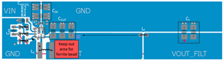
Place the second L-C filter, Lf and Cf , near the load to reduce any radiated coupling around the second L-C filter
Avoid placing the ferrite bead in the keep out region as shown in the figure below.
Place the FB resistors, R1 and R2, close to the FB pin and route the VOUT connection from R1 to the load as a remote sense trace. If a second L-C filter is used, this connection should be made after Lf.
The recommended layout is implemented on the EVM and shown in its User's Guide, TPS6291xEVM-077 User's Guide, as well as in the figure below.