This thread has been locked.

If you have a related question, please click the "Ask a related question" button in the top right corner. The newly created question will be automatically linked to this question.

TPS62912: TPS62912

Part Number: TPS62912
Other Parts Discussed in Thread: TPS62913

Hello TI support, 

I am thinking to use TPS62912 to get an precise supply voltage. I see from the data sheet that two LC filters would offer good ripple free DC. In my case I will have two boards one is power and the other one board should be powered by it. The data sheet suggests to put the second LC close to the load. It appears that I have to put this second LC close to the connector pin that connects the two boards as there is no space on the second board. I assume it should still work. I am wondering how in this case the placement of the first LC. Can I put the inductor in a distance from the converter? If I am using single LC filter, should I place output caps close to the load and the inductor next to the SW pin or should I move the both close to the load? 

Thanks for your  support

Olonbayar                         

  • Hello,

    Thanks for your question.  The primary LC filter should be placed close to the IC.  The layout recommendation is to keep the SW node very small, and this alone forces the inductor to be close to the IC. The output capacitor ground should be routed close to the PGND pin, so this will also keep the devices close. The secondary filter can be placed on the first or second board, but be sure to keep all parasitic inductances below the recommended 50nH that the device is compensated for. The FB pin is used for sensing the output voltage at the load, and would also need to be routed to be on the other side of the secondary filter (ferrite bead), so keeping it on the first board is most likely what you want to do. I recently posted a FAQ on layout guidelines for optimal ripple and noise performance with this device here: https://e2e.ti.com/support/power-management-group/power-management/f/power-management-forum/1066055/faq-tps62913-how-do-i-ensure-my-layout-results-in-the-best-noise-and-ripple-performance-possible-when-using-the-tps62912-and-tps62913?tisearch=e2e-sitesearch&keymatch=tps62913#

  • Hi Steve,

    Thanks for your replies. Great. One more thing to clarify. You say that:  

    The FB pin is used for sensing the output voltage at the load, and would also need to be routed to be on the other side of the secondary filter (ferrite bead), so keeping it on the first board is most likely what you want to do. 

    That means the ferrite bead needs to be placed on the board with the load or the power board. Can you please confirm it? I am thinking to get the feedback from the secondary LC output capacitor and then route it to the FB pin through a resistor. You mean here with the first board the power board or the load board? 

    I thought I would place both LC filters on the power board and put the secondary LC (ferrite bead and C7 and C8 as in the evaluation board) close to the pin header. There will be then no LC on the load board.       

    My connector would be simple 2.4 mm pin header. I think this header would not cause much change in the DC. Can you please suggest on that? Is it in this necessary to place the sec. LC on the load board?   


    Thanks for your great support


  • Hello,

    Sorry I wasn't clear with my response.  It seems your plan to have both LC filters on the power board and place the FB sense point after the ferrite bead near the header is a good approach. 

  • Hi Steve,

    Thanks for your reply. I have an another short question. For layouting the converter TPS62912, I am following the data sheet. There it shows that the last LC stage should be connected to the load by creating a copper area covering the components. It is not simple track and it is an area. In my design I have several such converters each of which is tied to loads that are close to each other. I can provide copper for every second LC. The same is applied to the wiring connecting the ferrite bead to the primary LC. My question is can I do these wiring with simple track maybe 0.4 mm without having having such copper area? What are these copper areas good for? 

    Thanks for your support 

    Olonbayart                                         

  • Olonbayart,

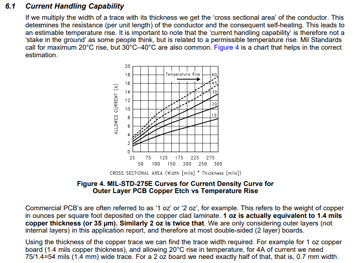
    The output voltage plane must be large enough to minimize thermal rise and the exact cross sectional area of the plane will depend on your application.  I recommend you look at section 6 of the Simple Switcher Layout guide since it addresses this question in detail.  See https://www.ti.com/lit/an/snva054c/snva054c.pdf?ts=1641911759206&ref_url=https%253A%252F%252Fwww.google.com%252F. The TPS62913 EVM uses 1 oz copper, and is not optimized for minimal area.  You can reduce the plane size based on your design from what is used on the EVM, but I don't think a 0.4mm trace would be sufficient.

  • Hi Steve, 

    Thanks a lot. I was trying to do PSPICE simulation for this component. I made bit change to the example provided in the download. For instance when I want to get 2.7V, I used the equation (8) for setting R2. I had to reduce R1 to 6k and 4k  so that I would get the resistor R2 below 5K as recommended. I did not do any other changes besides playing with  Sconf resistor. I could not get 2.7V and it is usually 2.3V. I am wondering where I made mistake. Would be great if you can comment on that?  I would need  several other even lower voltages (0.9V-2.7V) from this converter. In this case what would the variable I should set? 

    Thanks in advance 

    Olonbayar       

  • Olonbayar,

    Thanks for the question.  Did you change the load to reflect the new output voltage Note that the load is set by an equation R=V/I.  It may be hitting current limit if you did not do that.

  • Hi Steve, 

    That is great. It makes sense. I appreciate very much all the advices I am receiving from you. By changing the load resistance I can get the voltage I need. One thing to clarify is that my load would consume mostly around 150mA and when I do the caclulation for the load resistance for such current I get quite small load resistance which is 20 Ohm. With this load I get roughly 2.3 V not higher. By increasing the load to 3 kOhm I get 2.7V which I need. This implies the current consumption in this case has to be very very small so that I would have 2.7V. Is it the case? Can I use this component to power a device that consume 150mA-200mA at 2.7V. 

    Thanks again a lot 

    Olonbayar        

  • Olonbayar,

    Yes, a 150mA load is good.  You can see the efficiency curves in the datasheet that go down to that load level.