Hi,
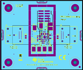
I looked at the user's guide of TPS7A94EVM-046,
The PCB Layout on page 5 and 6, I can't find out input BNC connector to
Device input connection.
I found device to J3-1,2 input trace has stub, so I guess input polygon pour is shelved on Second Middle Layer.
PDF pictures are not clear enough, if you can open the design file it could be better.
Thank you.