A related question is a question created from another question. When the related question is created, it will be automatically linked to the original question.
If you have a related question, please click the "Ask a related question" button in the top right corner. The newly created question will be automatically linked to this question.
Sure - I've run a bode plot of a 12V->3V design and I'm seeing a crossover frequency which is much lower than expected and would like to discuss whether this is expected and whether there any concerns about performance.
I'd prefer not to share schematics + results online so great if we could discuss further offline.
One further thought - could you confirm the correct procedure for measuring the TPS62913 control loop is as per section 2 in SLVA465A - i.e. you need to include the VO pin as well as the feedback network for the disturbance signal?
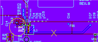
It's quite unclear from the eval board description what is actually happening here - there's no explanation as to how the traces being cut relate to the schematic and so it's hard to build a picture of what's actually changing.
Could you demonstrate in schematic form where the insertion resistor should be?
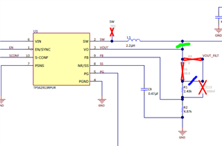
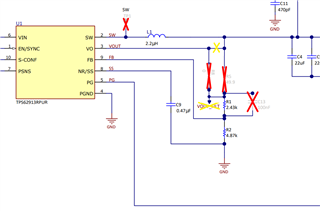
In the user guide Figure 5-1, you can see the location of R5 and R8 in the schematic. These components are not populated in the EVM when it is shipped.
Please see the snippet of schematic below where I have added marks to show where the trace cuts should be done on the schematic. The cut described in Figure 1-1 is shown with a blue mark below, and the cut described in Figure 1-2 is shown with a green mark. and don't forget to replace the ferrite bead with a 0 Ohm resistor for the most accurate stability measurements.
These changes allow you to inject a signal across the 49kOhm resistor as described in the user guide.
Thank you very much for the diagram although still not quite sure I'm following this. I've probably missed something so great if you could clarify:
The VO pin appears to have been cut from the VOUT net which makes sense but it's then been connected to VOUT_FILT via R8=0R. As FB1=0R, then VOUT_FILT=VOUT and so we're effectively connecting VO back to its original node (bar some elongated routing)?
Not sure if this is intended but I'm keen to make sure I'm measuring the loop correctly.
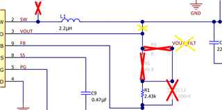
The trace cuts are effectively making the loop measurement using the FB sense node, as the VO connection is now connected to the VOUT_FILT sense point and not directly to the output of the inductor. The device has two feedback loops internally, with the VO sense being the AC loop and the FB sense being the slower DC loop response for the ferrite bead filter. Both loops can not be measured independently, so this give a way to measure the overall loop response.
I see what you are saying but surely VO is still connected to the inductor output given VOUT=VOUT_FILT (as FB1=0R)? I'm not sure we've changed anything with the VO trace cut with the exception of a small amount of PCB route?
For me taking the approach you've mentioned where VO=VOUT_FILT, I get suspicious results. I've just tried VO connected between R1 and R5 (in your above SCM snippet) and with this approach I get much more convincing results that are similar to the EVM plot but I don't want to continue with this method if you think it's incorrect?
Connecting the VO between R1 and R5 is essentially the same, except you have the drop across the 49kOhm resistor where the AC signal is being injected. The sense point, and hence the regulation feedback, is quite different when connecting VO to VOUT_FILT versus a short connection as originally on the EVM prior to the trace cut. Please verify that you cut the traces in the correct spots, and that you are injecting the signal across the 49kOhm resistor with the proper amplitude so that you are getting stable operation across the full frequency range. It is helpful to monitor the SW node during the sweep to see that the device does not go unstable. If it does go unstable during the sweep, lower the amplitude of the signal where it is unstable.
Thank you for your reply on this + on going support on this thread.
I've also run over the trace cuts myself - looking more closely at the SLVUBX2A EVM board datasheet and referring to the BSR077B EVM gerbers, I also agree we are cutting the trace between VO and L1 as you suggested previously. However, my read is that the other cut is actually disconnecting R8/C13 node from VOUT_FILT. The screenshot below shows that R5 is still connected to R8, R1 and C13 - I think this means we are actually cutting the R8/R5 node from VOUT_FILT as this is the long trace that connects after FB1 to the C7 output bulk.
I think this means we're doing something like this:
I suspect I'm still missing something as populating R8=0R would short out the insertion resistor R5 and the feedback network doesn't appear to now be connected to VOUT? It would be great if you could review and confirm if you agree with this.
If so, please could you review the correct test procedure and make sure we understand what's going on as I'm losing a lot of time on this and I feel this should be properly documented.
As a minor note, for benefit of others, could you also confirm you mean 49Ohm for the insertion resistor rather than 49kOhm?
To answer you last question first, yes, it is a 49Ohm resistor, not 49kOhm.
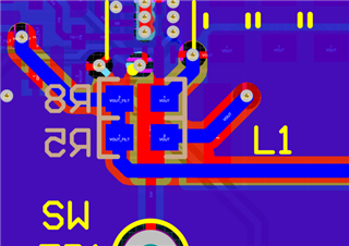
As to the VOUT sense, you can see on the bottom layer that installing the 0Ohm resistor for R8, it connects the VO pin feedback to VOUT through R5 (the 49 Ohm resistor). This moves the sense point to near the primary LC filter output caps C4 and C5. I see where my previous comment was confusing by stating VOUT_FILT, when the sense point is now closer to the primary LC filter and the VOUT_FILT sense point is not used, as you pointed out.
I can now see that the first trace cut is not only disconnecting VO from VOUT but also R8 from VOUT which isn't obvious from the schematic alone given the number of nets that connect to this node. I've tried updating the SCM to more accurately reflect the routing topology - I think the below makes it much clearer what is going on here but I'm open to your opinion here:
Please could you put in a request to have the EVM documentation updated to make this clearer. I'd also strongly encourage the EVM boards to have population options to prevent the need to do trace cuts if possible.