This thread has been locked.

If you have a related question, please click the "Ask a related question" button in the top right corner. The newly created question will be automatically linked to this question.

UCC5350: NMOS and PMOS ON timing between VCC2 and OUT

Part Number: UCC5350

Hello Support team,

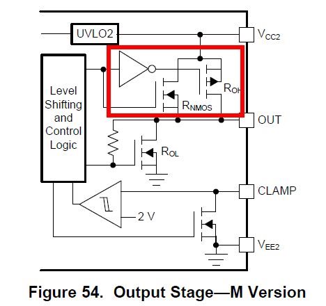
My customer ask NMOS and PMOS ON timing between VCC2 and OUT, is the on timing of NMOS and PMOS same?

Thanks,

Koji Ikeda

  • Hi, Ikeda-san,

    The operation of this circuit is discussed in section 10.3.3 Output Stage of the datasheet. If that doesn’t answer your question, can you please elaborate on your customer’s concerns? 

    best regards,

    Don

  • Hello Don-san,

    Thank you for you prompt response.

    Customer would like to clarify UCC5350 turn on behavior, because UCC5350 include NMOS and PMOS, while other vendor gate driver looks like to be simple.   

    Does the NMOS and PMOS start same turn on timing?

    NMOS looks like to turn on fast but turn off soon, due to no boost strap in IC, PMOS keep turning on, but,  the turn on speed is slower than NMOS? Is their understanding correct?

    If their understanding is correct, "The turn on-phase output resistance is the parallel combination ROH || RNMOS." on datasheet shows the behavior in initial turn on phase only, and to keep MOSFET high, PMOS only is used.

    Thanks,

    Koji Ikeda

  • Hi Koji, 

    Their understanding is for the most part correct. Both the NMOS and PMOS turn ON at the same time and are active during the switching transient. The PMOS does not take longer than the NMOS to turn ON.

    Both the NMOS and PMOS turn-ON during the switching transient of the power switch. Due to the gate driver not having a charge pump the NMOS is only ON during the turn-ON phase to support a higher drive current. Once the gate voltage rises the NMOS will turn-off leaving only the PMOS as the pull-up FET for the power switch. 

    Let me know if there's any additional question. 

    Best regards, 

    Andy Robles