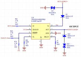
This thread has been locked.

If you have a related question, please click the "Ask a related question" button in the top right corner. The newly created question will be automatically linked to this question.

TPS1H200A-Q1: Help with TPS1H200A-Q1 Smart High-Side Switch

Part Number: TPS1H200A-Q1

Hi.
Please could somebody check the schematic below and say if there is something wrong or missing on it? Or if there is any recommendation?
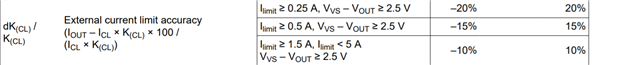
--> CURRENT LIMIT
Worst case... CL pin = 820 Ohms with -1% = 811.8 Ohms
Iout = (0.8 * 2500) / 811.8
Iout = 2.463A
2.463A * 1.1 = 2.71A (1.1 = 10% max tolerance for Iout >= 1.5A)
2.463A * 1.21 = 2.98A (it could be up to 21% tolerance for 3A max)

- The diodes B360A are rated for 3A continuos, and 60V.
- The TVS diode SMAJ36CA has a minimum breakdown voltage of 40V.

Questions:

(1) Since my layout is space limited, could I safely remove the 4.7K series resistors, R26 and R83, from pins IN and FAULT? My worry is that in case of damage on the transistor, my MCU coud receive high voltage on it's pins connected to IN and FAULT.

(2) This schematic is for use in a new project of automation module, so lets consider a very wrong installation on field done by the client. The power supplies used in the installations are 24V, so lets consider that the +24V is connected to the GND of the board, and that a GND wire is connected to the load output of the board, at 'OUT1-LOAD+' in the schematic above.

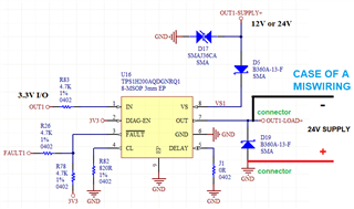
Doing this, the freewheeling diode will be directly polarized and will burn. So I also want to ask if there is another way to protect the circuit from reverse voltage of inductive loads, in a way that if such wrong installations be done, nothing get damaged, but please take into account that my PCB space for this circuit is limited.

Regards,

  • Hi Jeferson,

    Thanks for reaching out!

    I have several comments:

    1. For max current limit calculation, I think it will fall to 10% instead of 20% range as the current limit is over 1.5A.

    2. What's the purpose of the bi-directional TVS at Vs? Would uni-direction TVS work to clamp the voltage?

    3. Please be aware that the supply voltage will drop a bit due to D5.

    Regarding your questions:

    1. Yes it might be a concern as you pointed out. I would leave those in place to protect the MCU if you can (or find other places such as places close to MCU to protect it if the space around HSS is limited).

    2. What about a TVS in series with D19 rated above 24V (for example, 30V)? During inductor discharge, it will discharge with a negative voltage of 30V for a faster rate. During wrong connection situation, the TVS won't be conducting.

    Please let me know if you have additional comments or questions.

    Regards

    Yichi

  • Hi Yichi, thanks very much.

    --> Regarding the comments:

    1. Its Ok. I just wanted to have sure that current in the series diode, D5, will not reach 3A continous, 3A is the maximum continous current for it.

    2. The purpose of the bi-directional TVS at Vs is to limit possible voltage spikes to safer levels, and I did used a bi-directional one because if I use a uni-directional one it will also damage in some cases of miswiring.

    3. I understand that there will be a voltage drop at D5, but this is not a problem, I believe.

    --> Regarding the questions:

    1. I will keep the series resistors for pins FAULT and IN, I will find I way to route the PCB with them included.

    2. The use of an extra TVS in series with D19 is a good idea, but there is no enough space in the layout to include it. I will leave the circuit as it is in the first post. It will be responsibility of the clients to make the wiring of the installation correctly, and a diode like D19 is easy to make maintenance. I think to that to occur in practice a miswiring that will burn D19 there is a much small probability, but there is the possibility.

    --> New question:

    3. How about if I just modify D19 to a SMAJ36CA bi-directional TVS? Would the TPS1H200A-Q1 survive with inductive loads? (In practice, in the industry, we have seen power supplies delivering up to 36V, thats why the use of the SMAJ36CA).

    Regards,

    Jeferson.

  • Hi Jeferson,

    For the new question:

    If you are using clamp of 36V, depending on the bus voltage, the internal Vds clamp might kick it before the external TVS.

    If the internal clamp is used, then you need to make sure the inductive energy is within the spec.

    Please let me know if you have additional questions.

    Regards,

    Yichi

  • Hi Yichi, thanks very much.

    I will just keep the circuit of the original post. No any doubts...

    Regards,

    Jeferson

  • Hi Yichi.

    Now I see that there is enough space on the layout/board to add TVS diode in series with D19 (freewheeling diode), and much probably in practice I would use a TVS SMAJ24A(or CA), it has a minimum breakdown of 26.7V, maximum breakdown 29.5V, and maximum clamp voltage of 38.9V @ 10.3A. Do you think this TVS diode in series with the series schottky diode (D19) would be enough to protect the TPS1H200A-Q1 from reverse voltages of inductive loads?

    And also what you think of using in series with D19 a 27V zener of 0.5W or 1W, like these: 0.5W 27V zener and 1W 27V zener.

    Regards.

  • Hi Jeferson,

    The TVS diode approach should work in this case. About the Zener diode, I doubt if it can withstand the power if you have 2A current flowing through it and the voltage it tries to clamp is 27V.

    Regards,
    Yichi

  • Hi Yichi, thanks very much.

    Please check:

    I was thinking one thing, could I delete D19 and keep only D23?

    Regards.

  • Hi Jeferson,

    If a bi-directional TVS diode is used, you need to make sure the breakdown voltage will be higher than your bus voltage so it does not clamp your bus voltage in normal operation. Otherwise, a bi-directional TVS can be used and you can remove D19.

    Regards,

    Yichi

  • Hi Yichi, thanks.

    I think its better to use the bi-directional TVS than the diode, because using the diode in some case of miswiring it will be directly polarized and will burn, indenpendently of the supply voltage, while with the bi-directional TVS it will not burn when the voltage of the supply is lower than its minimum breakdown voltage, 26.7V. The power supplies of the machinery are 24V, it is not normal the voltage go over 26.7V, so the TVS solution would work for most of the cases.

    I could choose a bi-directional TVS with a higher minimum breakdown voltage also, but then the maximum clamping voltage would be higher also. For SMAJ24CA the maximum clamping voltage is 38.9V @ 10.3A, I think this value of 38.9V its better to be not increased, or could it be higher? If yes, is there an idea of the maximum voltage value possible? In order if it can be increased, the part number can be changed to one with a higher minimum breakdown voltage, in order the power supply voltage can go higher also.

    I think that for an inductive load, when it is switched off, the OUT pin of the transistor/IC could go up to -38.9V (negative), then could this damage the transistor?

    Regards,

  • Hi Jeferson,

    I would go with the 26.7V TVS. For 38.9V, it's likely that the internal clamp will kick in before the external clamp. If the inductor's energy is higher than the datasheet's spec then it might damage the part. Overall it would be a safer idea to go with 26.7 if the supply voltage stays below it during the normal operation as you mentioned.

    Regards,

    Yichi

  • Hi Yichi, thanks.

    Maybe I didn't understood well.

    The bi-directional TVS diode SMAJ24CA has a minimum breakdown voltage of 26.7V, and maximum clamping voltage of 38.9V @ 10.3A. So I think that in the worst case it will be seen a maximum negative peak voltage of -38.9V at OUT pin of the transistor when a inductive load is switched off, and I don't know if this could damage the TPS1H200A-Q1.

    I wonder if the internal clamp would trigger, because there is the diode D5 in series.

    Regards.

  • Hi Jeferson,

    Now I understand your point. If the clamping voltage is -38.9V, then the Vds will be 63V, and the internal clamp is likely to kick in before the TVS. Also why you think D5 will cause the internal clamp not working?

    In this case, I think there are two ways: One is to use single direction TVS + Schottky diode which use the TVS to clamp the negative voltage. The other is to rely on the internal clamp for inductive load.

    Do you know what would be the maximum energy the inductive load discharge will be? If it's less than the datasheet's spec then it will be fine. It also will save you one component.

    Regards,

    Yichi

  • Hi Yichi.

    For the solution you said with diode + TVS diode, the schematic would look like this?

    EDIT: this does not make sense for me, I can delete the uni-directional TVS that nothing will change.

    Regards.

  • Hi Jeferson,

    I would flip the direction of the D19 to clamp the negative voltage.

    Regards,

    Yichi

  • Hi Yichi.

    But then the voltage at OUT pin could go -38V negative also, same problem as before with the bi-directional diode.

    Please correct me if I am wrong.

    Regards.

  • Hi Jeferson,

    By using single directional TVS, you can choose a diode that clamps at lower voltages. It can't be achieved with bi-directional TVS as it will then limit the positive direction current in normal operation.

    Regards,

    Yichi