Dear Sir/Madam,
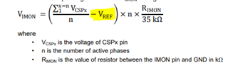
Page 130 of the TPS53667 datasheet states that the CSP traces be routed over VREF.
I am wondering why this is required?
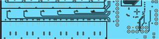
Can I route CSP and PWN signals between GND layers like shown below.
ie.
GND
CSP/PWN
GND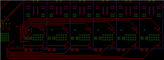
Regards Joe
Dear Sir/Madam,
Page 130 of the TPS53667 datasheet states that the CSP traces be routed over VREF.
I am wondering why this is required?
Can I route CSP and PWN signals between GND layers like shown below.
ie.
GND
CSP/PWN
GND
Regards Joe