This thread has been locked.

If you have a related question, please click the "Ask a related question" button in the top right corner. The newly created question will be automatically linked to this question.

UCC28911: Intermittent Operation

Part Number: UCC28911

Hello,

UCC28911 is used as follows:

VIN: 270V ~ 370VDC

VOUT: 14V/100mA x3 secondary outputs

Lp = 3.3mH

Lk = 31uH

NPA = 5.51

NPS = 6.96

Schematic is attached. 

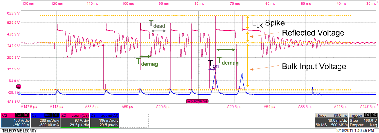
An Intermittent Operation is observed where the chip will work for a minute before it restarts. The following waveform shows a sudden increase in the primary current (blue trace) and an extended demagnetization period. I was wondering if that due to Lp = 3.5mH. 

What is Lp max UCC28911 can tolerate?    

I wasn't able to probe VS or IPK pins. The chip will act up when connecting a probe to those pins. What is the best way to probe VS? I tried a 5K series resistor with the probe but didn't make a huge difference. 


Thanks

WB

  • The schematic might be a bit confusing as it only shows part of the whole design. To clarify, the three outputs will drive high side FETs. REF_S3 is the +360V Input. 15V_S3 is sitting on top to drive n-ch FET. 

  • Hello,

    The VS pin is sensitive to capacitance and will cause the device to think it is failing input under voltage.  So you cannot probe it directly.  You need to probe the the aux voltage across the VS divider.    More than likely you are shutting down do to an OVP, OCP or input UVLO fault.The following will bring you an application note the describes primary side fault sensing, most common issues and how to resolve them.  https://www.ti.com/lit/pdf/sluaac5

    When it comes to selecting Lp you should choose a switching frequency greater than 54 kHz to get the full range of the control law.  This will determine what your Lp should be.

    Your bulk input voltage should not be spiking when the energy starts to be delivered to the secondary.  This would indicate that your design does not have enough input bulk capacitance.

    Your turns ratio Np/Ns seem to high it should be based on volt seconds and Dmax.  The Na/Ns should be sized to deliver 12 V to VDD.  If you were charging a battery you would probably design for a VDD of 20. You have a Na/Ns = 1.26.  So with a 14 V output you will have 17.8V.  So that is O.K.

    I reviewed the schematic and functionally it is correct. On first review the input capacitance and transformer turns ratio for this design is not correct. You can use the Webench tool that can be found on the following web page to size the transformer turns ratio correctly and primary magnetizing inductance.  I know this is for a single output but you can use it to calculate the primary magnetizing inductance, proper turns ratio, input and output capacitance.

    https://www.ti.com/product/UCC28911 , search on Webench:)

    Just need to do the following.

    1. Do a design for full input power.  This will give Lp, Np:Na:Ns and input capacitance, Rcs and VS resistor divider.

    2. Do the design for 1/3 of the power.  This will give you the output capacitance for each bank.

    Regards,

  • Hi Mike,

    Thanks for your feedback. The problem was solved. It turned out that the ground is bouncing causing UCC28911 to trip.