This thread has been locked.

If you have a related question, please click the "Ask a related question" button in the top right corner. The newly created question will be automatically linked to this question.

LM5026: LM5026 UVLO

Part Number: LM5026
Other Parts Discussed in Thread: UCC2891, UCC2892, UCC2893, UCC2894, UCC2897A

Hi E2E

When customers use LM5026 and refer to datasheet 8.2 and Figure 31, if they encounter problems with UVLO, please help to confirm and eliminate them.

As shown in the figure below:
Ch1: LM5026 VIN pin
Ch2: LM5026 UVLO pin
Ch3: LM5026 OUTA
Ch4: VDS of LM5026 OUTA Mosfet
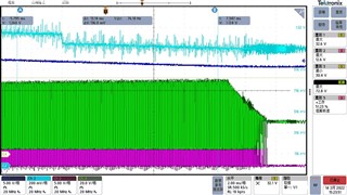
According to the LM5026 datasheet 8.2, when the UVLO pin is less than 1.25V, the IC will shut down. But the following Ch2 is lower than 1.25V, the OUTA pin still continues to output signal.

1. LM5026 spec why OUTA pin still output signal when UVLO pin is less than 1.25V.
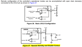
2. Can Vin be used as an ON/OFF signal? If you want to use the input voltage and protect it at 1.25V, please refer to Figure 27.
3. Description of MOSFET action mode in Standby mode between UVLO pin 0.4V~1.25V.
4. How to turn off OUTA and OUTB by controlling when the VIN voltage drops. Please provide suggested routes.
5. In addition, the Mosfet showed on the left as shown below, Q4B is P Mosfet, Q6B is N Mosfet. If you change Q4B to N Mosfet, is there any suggested route you can refer to?

  • Hi Rock,

    I've cop/paste each of your inquiries below and added my responses as bullet items for each:

    1. LM5026 spec why OUTA pin still output signal when UVLO pin is less than 1.25V.

    • 1.25V<V_UVLO<0.4V puts the LM5026 into standby mode. When V_UVLO is less than 1.25V, the soft-start cap is discharged by an internal 50-μA current source. As the soft-start voltage is falling due to the cap discharging, the converter is entering into a soft-stop operating mode (standby mode). Thefore, the converter will not immediately shut down when V_UVLO<1.25, if this is what is expected  

    2. Can Vin be used as an ON/OFF signal? If you want to use the input voltage and protect it at 1.25V, please refer to Figure 27.

    • If you want to use the UVLO pin for ON/OFF control, you must pull the pin below 0.4V. You can test this in the lab with the converter you now have, and observe is this is the behavior you expect.

    3. Description of MOSFET action mode in Standby mode between UVLO pin 0.4V~1.25V.

    • Once V_UVLO has exceeded the 1.25V threshold during start-up and then has decreased to 1.25V<V_UVLO<0.4V, the LM5026 remains enabled and re-start (1-μA restart vs 50-μA soft-start) will be activated when V_UVLO>1.25V, provided V_UVLO has not fallen below 0.4V.

    4. How to turn off OUTA and OUTB by controlling when the VIN voltage drops. Please provide suggested routes.

    • The important point for shut-down and restart is assuring the soft-start cap is properly discharged during shutdown. The only way I can see this happening in a controlled manner is by pulling V_UVLO<0.4V (0.3V is data sheet minimum).

    5. In addition, the Mosfet showed on the left as shown below, Q4B is P Mosfet, Q6B is N Mosfet. If you change Q4B to N Mosfet, is there any suggested route you can refer to?

    • No, for low-side active clamp you need the P-channel MOSFET so the intrinsic body-diode is pointing in the correct direction such that the resonant capacitance has the appropriate discharge path for establishing the conditions for ZVS. If you want to use a N-channel MOSFET, you need to consider a high-side active clamp. The differences between each are detailed here. Each configuration requires a different gate drive with unique protection features thoughtfully applied for each and this is what led to the development of the UCC2891, UCC2892, UCC2893, UCC2894, UCC2897A family of active clamp controllers.

    Thanks for connecting through E2E.

    Regards,

    Steve 

  • Hi Steve,

    Thank you for your answer, but for the second point, I would like to double-check.

    I have seen the datasheet for the UVLO instruction.


    But, what is the mean as the below show that can be shut down by forcing the ON/OFF input below 1.25V in the datasheet? What has the J2 source come from?

    Could you help to explain Figure 27? If remove the standby mode, the UVLO will shut done at 1.25V or 0.4V?

    Thank you and regards,

    Rock

  • Rock:

    • "But, what is the mean as the below show that can be shut down by forcing the ON/OFF input below 1.25V in the datasheet? What has the J2 source come from?"
      • Any low-impedance source capable of pulling U1-2 LOW can be applied to (J2) and used for ON/OFF control. If you use an active switch (NPN, NMOS, etc), you need to make sure the sat voltage is <0.4 (0.3V min). For testing in the lab, we may simply use a manual toggle switch to GND.
    • "Could you help to explain Figure 27? If remove the standby mode, the UVLO will shut done at 1.25V or 0.4V?"
      • Yes, if you remove the "STANDBY" MOS+Diode shown in Fig 27, you will have only ON/OFF control according to the "OFF" circuit shown in Fig 27. 
      • You have already shown by the waveform originally attached, what is the real behavior when V_UVLO<1.25V and we define this behavior in the data sheet as soft-stop. Since you have hardware, I suggest pulling V_UVLO<0.4V and record the waveform under the same condition. this is the best way to understand the response difference between V_UVLO less than 1.25V vs 0.4V.

    Regards,

    Steve M