This thread has been locked.

If you have a related question, please click the "Ask a related question" button in the top right corner. The newly created question will be automatically linked to this question.

TPS61199: Blinking LED

Part Number: TPS61199

Hi everyone,

I am writing to you because I have a problem with a new project that I am developing. following the instructions in the datasheet I made my circuit, but I have a problem, the LEDs on my LCD panel are flashing, the inductor and diode D1 heat up a lot.
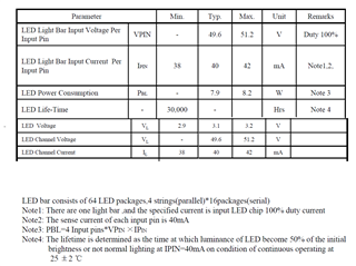
The power supply voltage is 12V and below the resistense and capacitor values.
The strange thing is that if I bring the power supply voltage to 13.3V the defect disappears and the LEDs stay on normally, and the inductor and the diode heat up less than before.
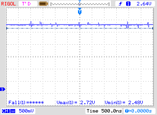
Below are the waveforms of Vout and OVP in the presence of the defect and after increasing the input voltage.
I ask you for support in order to solve the problem when the Vin is 12V.

Thanks
R2 = 162kOHM

R6 = 61,6kOHM

R5 = 301kOHM

R4 = 59,2 KOHM

C4 = 15nF

C5 = 270pF

Vout (with Vin 12V)
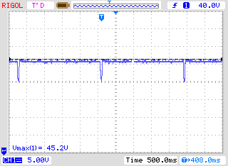
OVP (with Vin 12V)
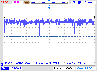
Vout (with Vin 13.3V)
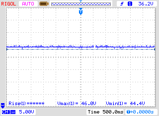
OVP (with Vin 13.3V)
  • hi pcb

       Can you help also provide the waveforms of SW, LED current?  It would be helpful if the schematic can be shared? or give the input voltage, inductor value

  • Hi Wang,
    the value of the inductor is 22uH, the input voltage is 12V. The scheme is that of the datasheet.
    Unfortunately I cannot provide the requested waveform because I have returned the circuit to the owner.
    However, I solved it, I no longer have the blinking of the led strips.
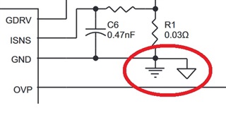
    In the application diagram presented on the datasheet, the gnd must be separated, and connected only near to pin 15.


    I cut my grounded track at the entrance to the circuit and reconnected it near pin 15.
    I checked the schematic of the evaluation board TPS61199EVM and the separation of the gnd is not there .....
    Was it just a coincidence or the mass track in its previous position made the operation unstable ??

  • hi pcb

        Per my understanding, it is necessary to connect these two GND nets together to form power GND reference for whole power circuit. One consideration is that R1 should be put near GND pin and the trance connecting R1 and GND should be short and wide. Also, TI recommends using short traces separate from power ground traces, connecting them together at a single point.

  • Hi Wang,

    thank you for your reply. Do you think it is possible to have a good routing of this circuit?

  • hi pcb

       Yes, you can follow the guide on layout in datasheet to improve the circuit.