This thread has been locked.

If you have a related question, please click the "Ask a related question" button in the top right corner. The newly created question will be automatically linked to this question.

TPS62840: Power consumption issues

Part Number: TPS62840

Hi,

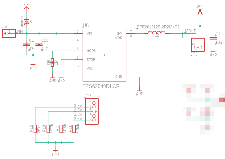
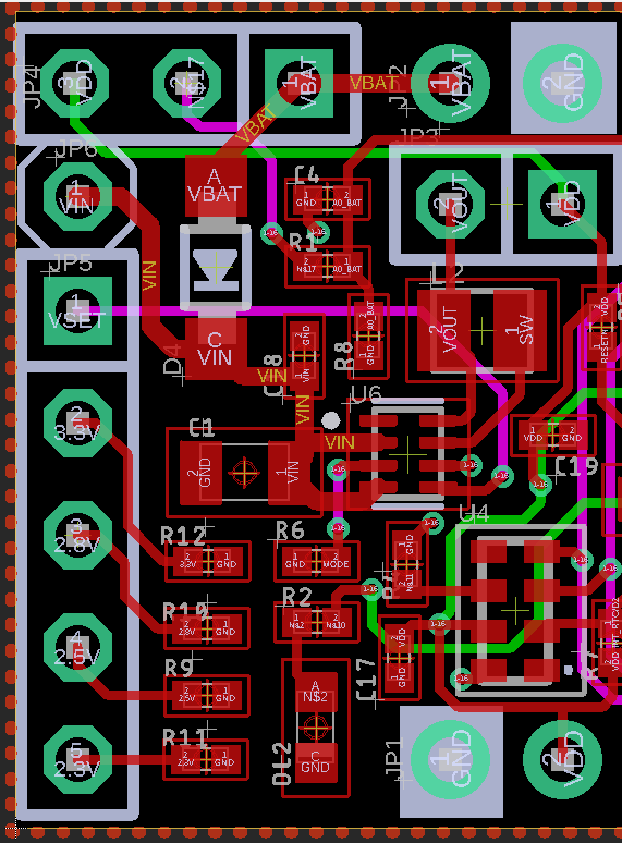
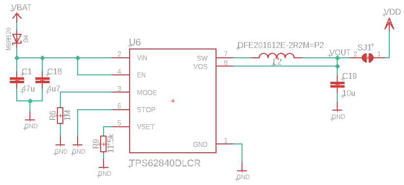
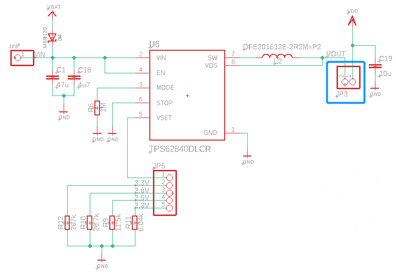
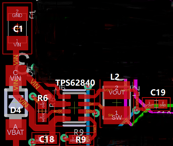
We want to use TPS62840 to convert the battery voltage to a fixed 3.3V or 2.5V to supply power for our load (an ARM-based processor). I used the TPS62840 evaluation board (TPS62840-1DLCEVM55) and it works very well with ultra low power consumption when the load current consumption is very low (several microamps).  When I designed a circuit according to the TPS62840-1DLCEVM55, it works but the power consumption is very high when the input voltage is a little higher than the output voltage.

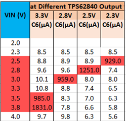
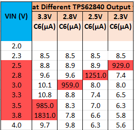
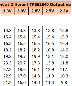
The left table shows the current measured by our designed board, the right one shows the TPS62840-1DLCEVM55 results.


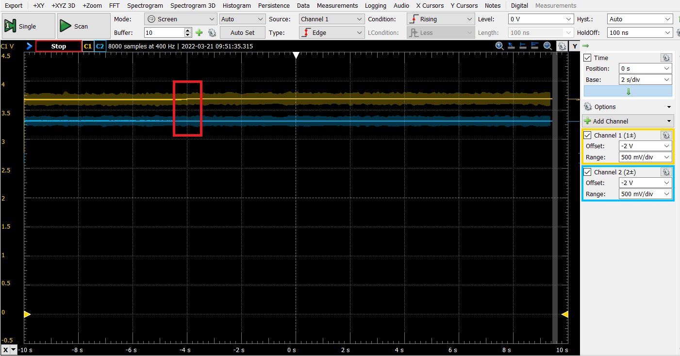
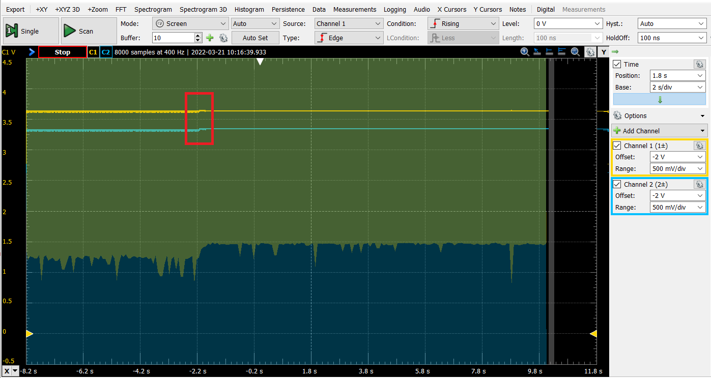
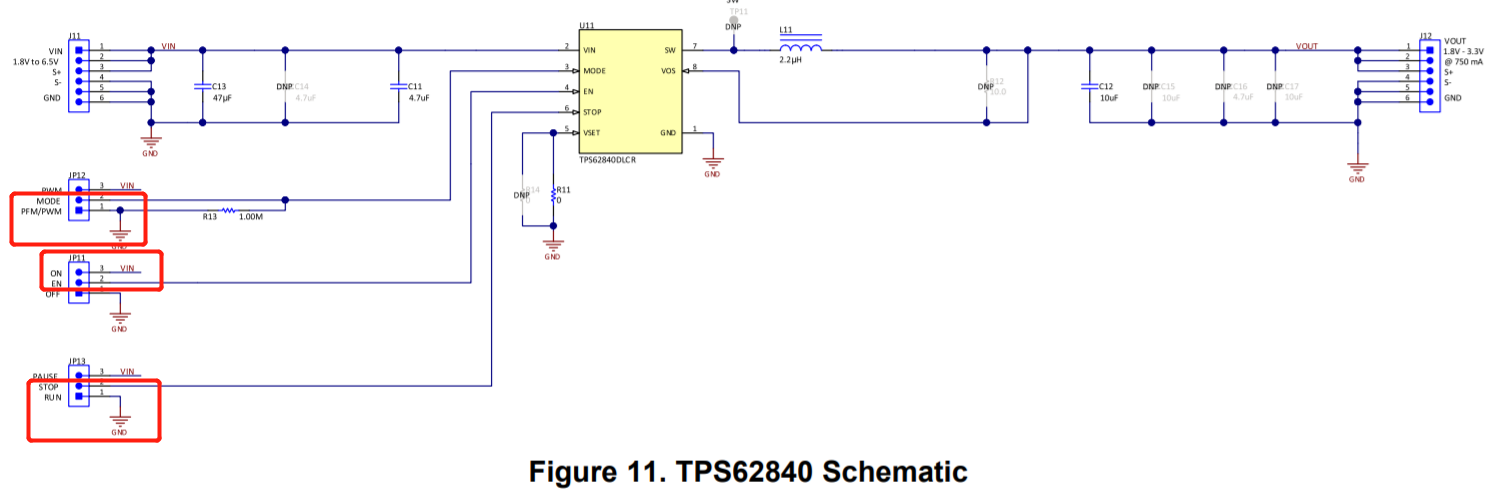
When we used the TPS62840-1DLCEVM55, the mode are selected as follows.

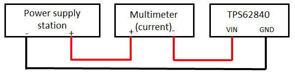
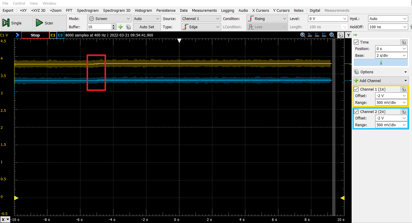
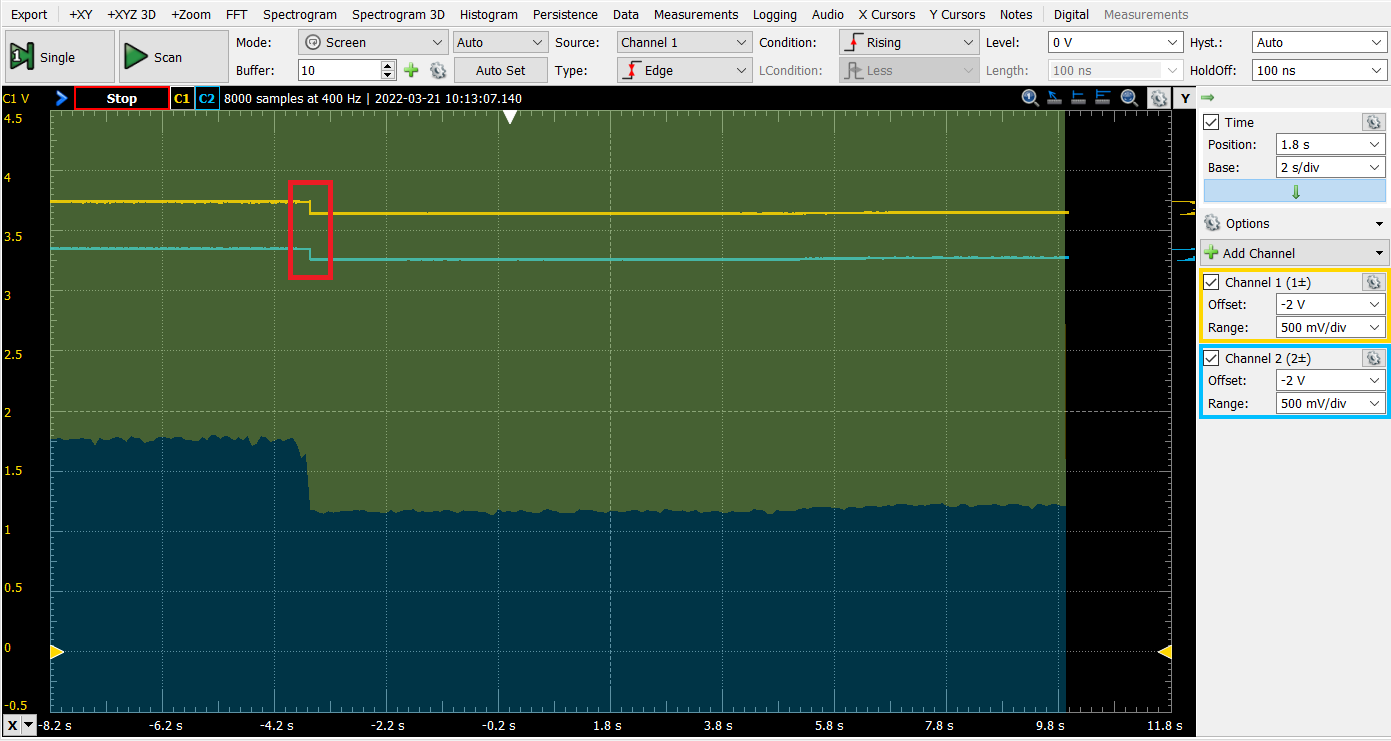
I confirm that the load state keeps absolutely same when we tested with thest two boards. The customer service suggested me to post my questions here. Could you kindly give some professional suggestions or comments to help achieve ultra low power consumption with this DC/DC converter? Thank you very much.

  • Hi,

    Please be informed that I am working on your request.

    I will review the above details and provide a feedback early next week.

    Regards,

    Febin

  • Hi,

    I reviewed the schematic and it looks fine.

    - Firstly, I would ask you to disconnect any part of the circuit that is connected to VBAT and VDD (except TPS62840). You can check the offset in the system by disabling the device and then you can re-measure the input current after enabling the device.

    - I could not find C6 in the schematic. Where do you measure the input current?

    Layout Review:

    - From the layout, it looks like the input loop is longer. Please place the input capacitor as close as possible to the IC and with a direct connection to the Vin pin. I would suggest to swap positions of R6 and C18.

    - Are all the resistors & capacitors connected to the GND pin of the IC?

    - If possible, please share the complete layout file.

    Regards,

    Febin

  • Hi,

    Do you have any updates to share?

    Regards,

    Febin

  • Hi Febin,

    I am sorry that I replied the email directly, but my answer did not appear here. I will update it again.

    Thank you very much for your professional response.


    - Firstly, I would ask you to disconnect any part of the circuit that is connected to VBAT and VDD (except TPS62840). You can check the offset in the system by disabling the device and then you can re-measure the input current after enabling the device.

    Maybe my description is not very clear. I powered from VIN or VBAT pins directly with a DC supply station. The multimeter was connected in series to measure the input current of the TPS62840 and our load device (the load device is powered from Vout of the TPS62840).

    Actually, I designed two circuits: one is used for testing, the other one is a simplified version.

    Version 1: for testing (when VOUT and VDD (VDD connects with our load) is connected, the DC converter supplies power for our load), the vin pin of the TPS62840 is connected to VIN or VBAT pins (via D4 to prevent reverse voltage).

    Version 2: simplified version. The VOUT pad is connected with the VDD pad directly.

    I measured these two versions, and each version has 5 boards. They all have this symptom: when the voltage feed into VIN of the TPS62840 is a little higher (0.1-0.3V) than the Vout voltage, the current dramatically increases (the load current should be low to microamps level). But with the TPS62840-1DLCEVM55, the measuring method and load conditions are exactly same, the total current is very close to 10uA.

    - I could not find C6 in the schematic. Where do you measure the input current?

    Sorry, there is no C6 on the PCB board as well. May I ask do you mean R6? The current measurement method was described previously.

    Layout Review:

    - From the layout, it looks like the input loop is longer. Please place the input capacitor as close as possible to the IC and with a direct connection to the Vin pin. I would suggest to swap positions of R6 and C18.

    Thank you very much for your professional suggestions. I will revise them in my next design.

    - Are all the resistors & capacitors connected to the GND pin of the IC?

    Yes, I think so. There are no errors. All GNDs are connected with the copper polygon, including the GND pin of the IC.

    - If possible, please share the complete layout file.

    Sorry Febin, I am afraid our company cannot allow me to share it.

    Hope my description is clear and helpful to solve my problem. If you need any more information, please feel free to let me know.


    Thank you so much for your kind help.


    Kind regards,

    Xiaoli

  • Hi Xiaoli,

    Thank you for all the information. 

    So, I think I understand the problem now. The additional input current drawn by the system is probably because of the transition from 100% mode to normal mode and then toggling in this transition for a while. 

    Could you please share the scope plots for Vin, Vout, Inductor current and SW node during this event. I think we will see higher output ripple as well during this event.

    What is the maximum load on TPS62840 for the below measurements?

    For the EVM measurements, was any load used?

    Regards,

    Febin

  • Hi Febin,

    Thank you very much for your prompt and professional response. Unfortunately, I measured all values with the multimeter, so there are only average values avialble as shown in the tables.

    The load of TPS62840 never changes. If TPS62840 was not applied, the load is directly powered, the current is around 10 uA (it's based on the input voltage, the higher the voltage, the lower the current).

    For the EVM measurements, the load is same. It can be regarded that the load never changes,

    1) Without TPS62840 and EVM, the load is directly powered, the current is around 10uA.

    2) With EVM to power the load, regardless of the input voltage, the current is a few microamps higher than 1), i.e.,10+uA.

    3) With our design board, i.e. using TPS62840 to power the load, the current is same as EVM when the input voltage is much higher than the output voltage of the TPS62840. But when the input voltage is only 0.1V-0.3V higher than the output voltage of the TPS62840, the current is much higher than 1), i.e., around 1mA. But with EVM, the current is always very low, only 10+uA. We designed the board according to the EVM schematic.

    We need an ultra-low power consumtion design. 1mA is too high for this load. But when we evaluated the power consumption with the EVM, it really works.

    Hope my description is clear. If you need any moe information, please feel free to let me know. Thank you so much.

    Kind regards,

    Xiaoli

  • Hi Xiaoli,

    Thank you for all the information. 

    We would need the scope plots for Vin, Vout, Inductor current and SW node to understand the behavior of the device during this event. Unfortunately, we cannot get further with multi-meter values. We need the scope plots only for the test conditions marked in Red. 

    It will also be really helpful, if I can get the complete schematic. If you have problems sharing it here, we can always go offline and discuss through direct Emails.

    Regards,

    Febin

  • Many thanks, Febin.

    I will try to measure the scope plots next week.

    Unfortunately, it is not allowed me to share the complete schematic. But I confirm that the load is only connected to VDD. The following schematic is the complete design for TPS62840. Case 1) was measured when JP3 is open and the power was directly supplied from VDD. Case 3) was measured with JP3 closed and the power was supplied from VIN or VBAT.

    I will update the scope plots next week. Thank you so much for your kind help. Have a wonderful weekend.

    Kind regards,

    Xiaoli

  • Hi Xiaoli,

    The schematic for TPS62840 looks good. I wanted the system schematic. Nevertheless, please share the scope plots.

    Regards,

    Febin

  • Hi Febin,

    Thank you very much for your pormpt response. I measured some scope plots and hope they will be helpful.

    Load condition description: the load status changes from working (generally the current is from 4 to 7mA) to sleeping (generally should be microamp level). The red rectangles show the voltage at the status transition.

    Test1: input voltage is 3.7V, output voltage is selected as 3.3V.

    Current measured with the multimeter: working (4.8mA), sleeping (1.59mA, the results is similar when the 3.3V<VIN<3.7V, the sleeping current decreases with the VIN decreases).

    Voltage measured with Analog discovery2: CH1(yellow line, VIN), CH2 (blue line, VOUT):

    The SW pin voltage was directly measured by using the red rest lead to contact the inductor pad (SW connected side).

    But the mutimeter shows that current increases when the test lead contact the inductor pad: work (5.35mA), sleep (2.18mA).

    CH1 (yellow, VIN), CH2 (blue, SW):

    Sorry that the inductor current is hard to measure.

    Test 2: input voltage is 3.8V, output voltage is selected as 3.3V.

    Current measured with the multimeter: working (5.02mA), sleeping (20.4uA).

    Voltage measured with Analog discovery2: CH1(yellow line, VIN), CH2 (blue line, VOUT):

    The mutimeter shows that current increases when the test lead contact the inductor pad: work (7.02mA), sleep (2.71mA).

    CH1 (yellow, VIN), CH2 (blue, SW):

    Another discovery is that when I disconnect VOUT and VDD (via disconnecting JP3), which means the TPS62840 does not connect with any loads (our load is powered with the VDD pin), the current (measured by mutimeter) increases from 1.61mA to 1.93mA when the VIN increases from 3.3V to 4.00V. But when I measured with the EVM board, without any load connection, the current is only 2~4uA. 

    Thank you so much for your kind help.

    Have a good day.

    Kind regards,

    Xiaoli

  • Hi Xiaoli,

    Unfortunately, the time scale used is too large to analyze.

    Could you plot the same in 'us' range?

    Regards,

    Febin

  • Hi Febin,

    Thank you very much. I apologise for the wrong scales. I update some plots in a document and attach it here for your reference. Unfortunately, the recorded values in excels have low resolution, which may be not helpful. I put all images in the word file. If it needs to be more scaled, please feel free to let me know.

    Many thanks for your kind help.

    Analog Disc.zip

  • Hi Xiaoli,

    I am Out of Office today. I will get back to you tomorrow.

    Thanks in advance.

    Regards,

    Febin

  • Hi Xiaoli,

    I think there is a system load that is pulling current from the TPS62840. Without a full schematic and layout, it is not possible to find the root cause. And you also confirm that on the EVM, the input current is very small. So, it is definitely related to your system design.

    Please do the following:

    Disconnect the load (processors and/or any other load) at VDD from the below design and connect a power supply instead of the battery at VBAT.

    Restart the system. 

    Please measure the input current.

    Observe the switch node to confirm that the device is in PFM. 

    Please do not use the other board. We need to go step by step to find the root cause.

    Please be informed that I will be OoO this week and will be back on Monday. Please expect a delay in my response.

    Regards,

    Febin

  • Hi Febin,

    Thank you so much for your kind help. I will try to update the information on Friday.

    Additionally, my manager agreed to share the schematic with you offline. Could you share your email with me at your convenience? Thank you so much.

    Have a wonderful day.

    Kind regards,

    Xiaoli

  • Hi Xiaoli,

    Please send to febin.hameed@ti.com

    Regards,

    Febin

  • Hi Xiaoli,

    As we are discussing this issue offline, I will go ahead and close this thread. I hope you are fine with that.

    Regards,

    Febin