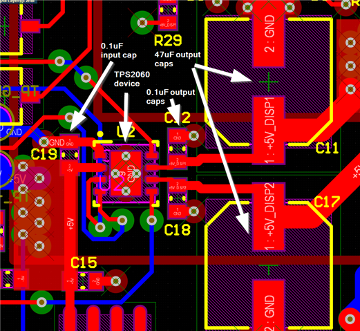
We have been testing the TPS2060DRBT device as a 5V power switch on a new design and have had two instances where after only light bench work these parts have become damaged.
Here is the configuration: We feed 5V to the input and selectively turn on the two output channels which feed other circuits. Enable lines and fault lines are all directly tied to a microcontroller powered at 3.3V. There is a 0.1uF ceramic cap on the input supply lines and the two output lines. Additionally, there is a 47uF aluminum electrolytic on each of the outputs. Output lines are tied to a pair of connectors that lead to other downstream boards powered from the outputted 5V lines.
Once the part is damaged, we observe 5V present at the input (pin 2) but 3.8V at both the two output pins (7 and 8). Additionally, the enable lines are both sitting at 3.48V DC even though the microcontroller is configured for a push-pull output on both enable lines (implying the enable lines are perhaps back feeding the I/O protection diodes of the micro and clamping at 3.48V). The fault lines (pins 5 and 8) are both sitting at 3.57V DC. Fault lines are connected to micro pins configured as inputs. The part also gets slightly warm to the touch in this state. When powered down, the impedance of both output pins to ground is several megaohms just as it is looking at an undamaged board.
At the time the damage occurred, no excessive loads were being drawn on either output, and the application software had channel 1 enable asserted on and channel 2 off.
What is interesting to me is that both channels appear to be damaged in the same way - not obvious that it would happen that way looking at the datasheet diagram which makes it appear no structures are shared other than the under voltage lockout block.
Can you help me understand what the likely cause of this damage is?


