This thread has been locked.

If you have a related question, please click the "Ask a related question" button in the top right corner. The newly created question will be automatically linked to this question.

UCC24612: UCC24612-1DBR

Part Number: UCC24612
Other Parts Discussed in Thread: UCC256301, TIDA-010015

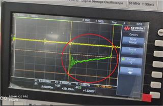
I am using LLC (UCC256301)  topology for output 24V / 20A and using UCC24612 for output stage.

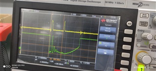
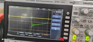
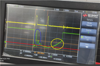
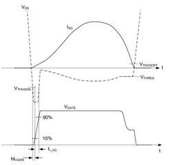
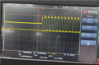
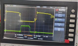
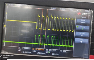
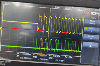
When Bulk voltage is 340 Volts, gate pulses of synchronous rectifier are present. But as soon as Bulk

voltage increases to 368V, gate pulses of synch rectifier stops. What could be the reason.

Regards 

Pravin Khisti

  • Hi, Pravin:

    Thanks for reaching us. 

    UCC24612 senses the Drain voltage to determine the gate pulse on/off, thus, would you please share me the VDS, VGS and VREG waveform to me for reference?

    The Vthgon is -240mV and Vthgoff is -9mV, thus, it needs to zoom  in to check each waveform and see the signal is correct or not. 

    Please check the waveforms as Vbulk at 368V and 340V. 

    Since LLC's switching frequency varies with input voltage, and I think it can be something happened when fs increased. It would be more clear after checking the waveforms. 

    Btw, if you do not mind, please share me the schematic for reference. Thank you very much. 

    Regards, 

    Wesley

  • Hi Wesley,

    We are using TIDA-010015 design as it is.

    Please refer below the wave forms

    When bulk voltage is 350V Yellow is Gate pulses To mosfet and Green is Vgs

    When bulk voltage is increased to 390V Yellow is Gate pulses To mosfet and Green is Vgs

    Please let me know if you need further details

    Regards

    Pravin Khisti

  • Hi, Pravin:

    Thanks for your feedback. It seems your Vds is wired both at 350V and 390V input.  And even the operation is incorrect as 350V input.

    Vin=350v

    As you can see as below, VDS rings back to positive and gate pulse stops immediately and turned on again after Toff blanking time. 

    However, the slope in yellow circle is strange. Compared the figure as below, the VDS should not rise with this slow slope. 


    Another wired point is the VDS is only 15V around, based on the TIDA-010015. The VDS should be higher than 24V.  Would you please check it again? If the VDS is only 15V, the output might not be 24V. Please also check UCC24612-1's VDD and VREG. And you may need check the LLC operation is correct or not if the waveform is true. 

    Vin=390V

    It has similar questions to me.  The max VDS voltage is only 1.5V. I think it should be incorrect. Maybe it is caused by oscilloscope's limitation. However, he VDS shape is like a CCM flyback, not LLC. Would you please check the measurement is correct or not?


    I thought the VD does not get the correct voltage signal from the MOSFET to make this kind of issue. So please check current waveform if the measurement is correct and make sure VDD and VREG is stable to enable UCC24612 first. 

    Please share me your investigation and we could discuss how to fix it. 

    Thanks. 

    Regards, 

    Wesley

  • Hi,

    Thanks. I will check and revert.

    Regards

    Pravin Khisti

  • Hi,

    VDD is 14.5V, VREG is 16.5V. Output voltage is 24V Stable.

    Below is VDS wave form (Yellow).

    I tried to tune snubber of SR but ringing wave form is unaffected.

    LLC is working and have sine wave form. 

    I do not have current probe. Is any other way I can measure current waveform of VD.

    Reagards

    Pravin Khisti

  • Hi, Parvin:

    The waveform seems better and clear. May I know what's output current at this test condition?

    Since you can see the bottom of VDS is still ringing, and not always in negative side. If current is sinuous, the bottom of VDS should be sinuous because Vds=Ids * Rds, and the Vds does not switch all the times. I think it may operates as light load. If yes, please increase the output loading to make sure the Vds is negative when current flows to MOSFET drain-source. And check if the gate pulse activate. 

    The VDS ringing mostly comes from the IDS and stray inductance on PCB. It would be improved to reduce the distance between IC VD and MOSFET Drian. So does IC VS and MOSFET Source to get more accurate VDS signal. Also, a shortest loop measurement is helpful to check if the noise is real or not. 

    Please share me if it is helpful to your situation. 

    Regards, 

    Wesley

  • Hi Wesley,

    Thanks for the help. All waveforms I uploaded previously are without any load. Below are the wave forms with 3A output load.

    Yellow is VGS and Green is Gate pulse.

    Out of 16 pulses 4 are as expected for output current 3A. Will other take  ideal shape with increasing load current?

    Regards

    Pravin Khisti

  • Hi, Pravin:

    Yes, I think gate pulse would get normal as load increased. As you can see as below, the VDS goes positive and gate pulse width shrink.

    So the operation is expected so far. It should operates normally once LLC operates in symmetric mode instead of burst mode.  

    Regards, 

    Wesley

  • Thanks for all the support.

    Regards

    Pravin