This thread has been locked.

If you have a related question, please click the "Ask a related question" button in the top right corner. The newly created question will be automatically linked to this question.

TPS62827: TPS62827A Switching Waveform

Part Number: TPS62827


Hi Team,

The customer are evaluating of using TPS62827A DC-DC as the alternative candidate for TPS62827 in current product due to shortages.

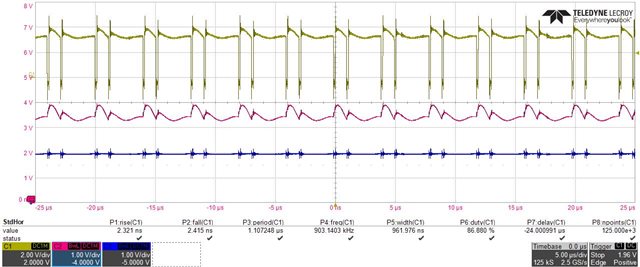
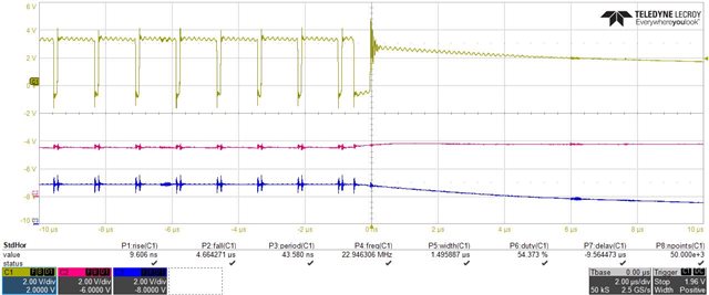
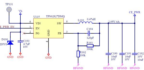
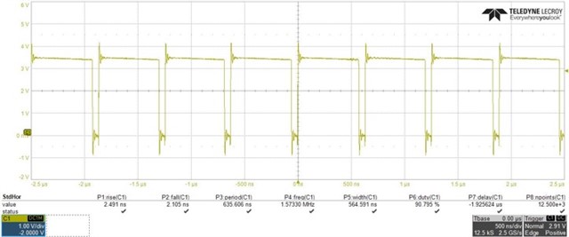
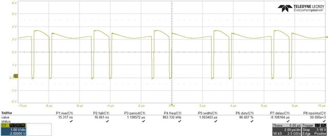
Please reference the switching waveform of these two DC-DC and the schematic as below.

For TPS62827A, the switching waveform seems irregular when we try to operate at 4A and low input voltage of 3.4V. We are not sure if this could lead to instability or you think this is a normal behaviour that we should not worry. Thank you.

TPS62827 Switching waveform (Input 3.4V, output 2.9V, I load = 4A)

TPS62827A Switching waveform (Input 3.4V, output 2.9V, I load = 4A)

Best regards,

Mike

  • Hi Mike,

    Can you share the PCB layout around the TPS62827?  The output caps are grounded to a different net than the IC and input caps.  

    The second waveform is operating at a lower frequency as well.  Can you share the waveform at 2A and 3A?  If this is with an electronic load, can you test with a resistive load instead?

    What is the part number of the inductor that you are using?  Is it possible to put a wire in series with the inductor and share the waveform from a current probe to see the inductor current?

    Thanks,

    Chris

  • Hi Chris,

    Thanks for the reply, the customer connect the output caps gnd and IC gnd with the big ground plane. You can regards they are the same gnd.

    For the inductor part number, they are using the one which we suggest in DS - TFM201610ALC-R47MTAA, TDK.

    For the inductor current, it is hard to capture for the customer.

    We also change the input to the TPS62827A DCDC using battery instead of power supply.

    It seem that the output shutdown instead of the abnormal SW waveform.

    The abnormal SW waveform due to cabling of the power supply that affecting the Vin?

    Below is the waveform for both power supply & battery.

    Note: the load have change to R mode. Ch1 is SW, Ch2 is Vin, Ch3 is Vout

    Vin connect to power supply

    Vin connect to Battery

    Best regards,

    Mike

  • Thanks for sharing the additional waveforms.

    It is critical how the input voltage is supplied.  Since Vin is very close to Vout, any additional voltage drop (from wires, connectors, etc.) will greatly affect the observed behavior.  How is Vin applied in the real application?

    You can try adding additional input capacitance on the PCB to try and stabilize Vin and overcome the impedance of the input supply.

    How does the waveform look with a lower load?

    It should still be checked with a resistor load instead of an electronic load in its resistive setting.  In many cases, an electronic load affects the circuit's behavior due to the load's control loop always changing to try and maintain the setting.

    Chris

  • Hi Chris,

    Thanks for the feedback, the Vin is supply by battery in the customer real system. The waveform of Vin is captured near the device.

    Since the customer is adding 4.7uF as input cap, is there any recommended value?

    For the lower load waveform, I am still asking the customer to provide, will keep you in the update.

    For the resistor load, I will check with the customer whether they can help to do this on bench test.

    BTW, another question from the customer is that the different heavy load switching frequency between TPS62827 and TPS62827A.

    It seems that the switching frequency of TPS62827A is lower than TPS62827 in 4A application. 

    Will the lower switching frequency cause the switching waveform looks abnormal? Is there any potential issue, if the customer go production with TPS62827A? Thank you.

    Best regards,

    Mike

  • Hi Mike,

    No, there is no issue if the frequency changes.  3.3Vin to 2.5Vout is a high duty cycle where the frequency can depend on a minimum off time as explained here: https://www.ti.com/lit/an/slyt646/slyt646.pdf This minimum off time can vary from device to device.

    I recommend adding a 100uF ceramic on the Vin net and see if this helps/changes things.  The required capacitance value depends entirely on the impedance of the battery, connector, wiring, etc.

    Chris

  • Hi Chris,

    Thanks for helping on this case, the customer is still working on the bench test. I will keep working with them, if there is any further question, I will create another post.

    Best regards,

    Mike