This thread has been locked.

If you have a related question, please click the "Ask a related question" button in the top right corner. The newly created question will be automatically linked to this question.

UCC28712: Startup Issue

Part Number: UCC28712

Hello -

We are attempting to startup our flyback power supply but are running into issues. We are using the UCC28712 controller.

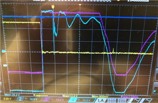
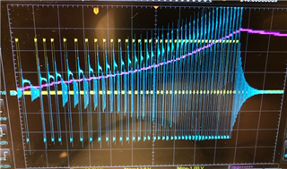
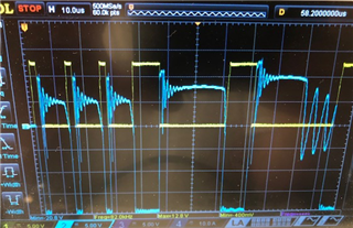
We see Vdd charge to ~ 21V and then the gate pulses 1 time.  The pulse width of the gate signal is ~ 250ns.  The amplitude is ~ 13V.  

Vdd then discharges over ~ 20ms and the process repeats.  Any thoughts on what is going on?  Why does the gate signal shut off at 250ns?  Why don't I see 3 pulses?

Thanks for your help!

Brett

  • Hello Brett, 

    Thank you for your interest in the UCC28712 flyback controller.

    The narrow gate pulse (~250ns) is usually indicative of the voltage at the CS input exceeding 1.5V, which may have more than one cause. 
    Please refer to these debug aids to help find the problem and solve it: https://www.ti.com/lit/an/slua783/slua783.pdf  and https://www.ti.com/lit/pdf/sluaac5 .

    To your point, we do usually expect 3 sequential pulses to result in a UVLO-cycle shutdown. It may be possible that when you zoom out to view the VDD cycling, your sampling rate cannot resolve the three separate pulses and it displays as only 1 pulse.  When you zoom in to measure the pulse width, the other pulses are far out in time and not visible. 
    If your oscilloscope is capable, I suggest to set the sweep rate at 10us/div and set the sampling to at least 20ns/point.  Hopefully at least 2 of the 3 pulses will be visible on screen. 

    Regards,
    Ulrich

  • Hey Ulrich - you were correct. It was shutting down due to over current. We had the wrong current sense resistor (909 Ohm vs 0.909).  Changing the resistor helped.  We now see the 3 gate pulses, but it still shuts down. Vdd looks ok.  It holds out for about 10ms.  The aux voltage during the MOSFET on time looks ok (above the UVLO condition).  The voltage across the current sense resistor is not linearly rising as expected.  I'll try to get a screen shot today.  It appears very noisy so not sure what i am seeing but it doesn't look like normal current rise through an inductor.  Would the Rls resistor cause this?  I know layout could cause this but I don't think that is the issue (at least not on 3 pulses).  Anyway thanks for your quick response above.  And if you have further suggestions they would be appreciated.

    Brett

  • Hello Brett, 

    I'm glad you were able to find that bug and make a little progress.

    Meanwhile, the shutdowns maybe due to any of several symptoms, the simplest being insufficient input voltage for start-up. That level depends on what voltage you are providing, the turns ratio and the Rvs1 value.  
    Please refer to one of the PSR debug guides that I listed earlier to help track down the problem and solve it. 

    Meanwhile, when providing the waveforms, also please identify each trace, provide the operating conditions (input voltage, load condition, etc) and design details like the values around the controller and the transformer parameters.  That will save time from having to request missing information. 

    Regards,
    Ulrich

  • Hey Ulrich - we got a litter further yesterday.  The device starts up and runs until Vout exceeds the over voltage trip point.  

    Here is a screen shot showing the last switching cycle before over voltage shutdown.  Output voltage is shown in dark blue.  Secondary voltage from transformer is shown in magenta. Light blue shows aux voltage from transformer.  And yellow shows the gate voltage.

    This next shot shows the entire cycle from startup to shut down. Yellow is the gate voltage. Light blue is the aux voltage from the transformer. And magenta is the output voltage.

    The output voltage is designed to be regulated at 24V.  We see the shutdown occurring at around 30V which is consistent with the over voltage trip calculations.  When we changed Rs2 (increased), we saw the over voltage trip point go down which was expected.  This seemed to confirm the device was shutting down on over voltage.

    A couple observations/questions.

    1. Increasing the load resistance and/or increasing the output capacitance did not help.  The time until over voltage increased but still got same results.  

    2. During startup it was common to see the switching occur at peak voltages.   Here is a close up taken just after startup.  Yellow = gate voltage. Light blue = aux voltage.

    The 4th transition looks ok and the 5th looks like the valley was missed.  Now this is still in startup so i am not sure if this is normal or if it indicates a problem.  In the shot with the full cycle, the missing valley cycles seem to go away once output voltage gets above ~ 15V.   

    3. The last observation is Ton keeps increasing until shut down. You can see this in the full cycle shot above where the spacing between the yellow pulses get closer as Vout gets higher.  This probably explains why Vout keeps increasing. The shot below shows Ton at about 9us and Toff at 6us.  Yellow = gate voltage; Magenta = Vout; Light blue = aux voltage.  

    Para 2.7.1 in SLUA783 talks about the drain node capacitance being too high may be the cause of what I am seeing.  Is there anything I can do to verify this is the cause of what I am seeing (short of a redesign)? 

    Any other suggestions?

    Thanks for your help.

    Brett

  • Hello Brett, 

    I'm glad it is starting up, but I'm concerned that it doesn't achieve regulation. 

    My comments to your observations: 
    Obs 1:  This is expected.  Once the power stage reaches the Iocc limit, it simply takes longer to charge up a larger output cap, or the same cap with a higher load on it (the load current diverts from charging up the cap).

    Obs 2:  Since start-up is transitory, some missed valley switching is not a major concern.  There is complicated internal timing going on that I don't fully understand myself that can account for these missed valleys.  Sustained misses in steady-state operation is another issue, but we don't know at this time if you will see that or not. If it does, there is a reason which I do understand, but we'll deal with it then. 

    Obs 3:  Ton is not actually increasing much cycle by cycle.  It is the demagnetization time that is decreasing, because the reflected voltage from Vout is increasing and the time to demagnetize the transformer becomes shorter each cycle.  The constant-current mode regulation of the UCC28712 maintains a demag-to-period ratio of 0.425 (the Kcc factor). 6us out of 6+9us = 6/15 = 0.4 is pretty close to Kcc (the 6 and 9 us numbers are roughly estimated).
    Peak-current dithering for EMI reduction kind of complicates the timing.

    The demag time waveform on the last photo has very large ringing on it.  This indicates a lot of winding capacitance ringing with the magnetizing inductance. 
    I am concerned that this ringing interferes with the proper sensing of the demag knee at the VS input which is necessary for correct regulation.  This may account for why the OVP is up at 30V (125% of 24V) rather than the expected 27V (113%).  But it doesn't explain why it simply does regulate at 27V then.

    How can it miss the knee for regulation, yet detect the overvoltage (although at a higher point)?  The device does measure for OV twice each cycle, first just after the tLK_RESET time (~2us) of datasheet Figure 15, and second at the demag knee point.  It discards the first measurement when it gets the second.  If VS cannot detect the knee, then it is probably acting on the first reading.      

    That suggests that the signal at the VS pin may have excess capacitance on it which is rounding off the knee point too much and it can't regulate.  OVP is acting off of the first measurement, which would also be distorted by capacitance on VS which may account for why OVP is higher than expected. If you have a physical capacitor on VS, please remove it.  

    If no cap, there still may be excess stray capacitance from a long trace(s) from the VS pin to the resistor-divider pads, especially if you have it over a GND plane.  Please compare your layout to that of the Layout Example of Figure 30. The goal is to minimize node-capacitance on VS as much as possible.   
    Also, the transformer design needs a review to eliminate the low-frequency ringing seen during demag.  High-freq ringing after the leakage spike subsides is normal, but the demag ringing seen above is not usual. 

    Regards,
    Ulrich