


Hi Team,
Could you please help me with below questions? Thanks.
1,When doing single-point grounding, which point should be the GROUND? I think using the source of the MOSFET as the ground point can reduce the area of the driving loop. Any comments here?
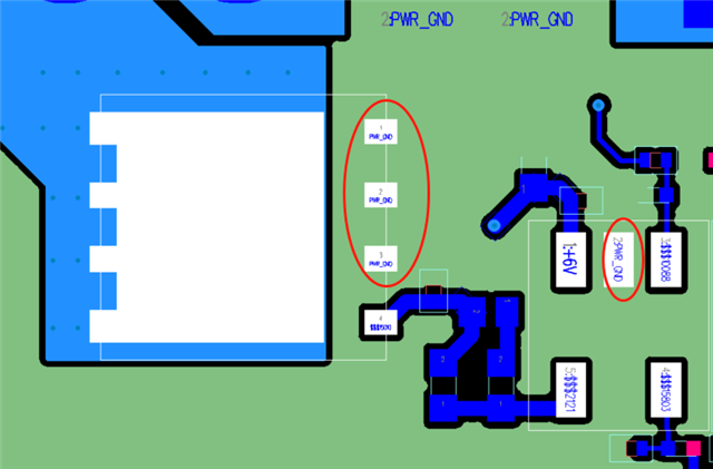
2,Figure 1 is the recommended layout from datasheet. The customer does not have the line marked by the red note, but uses a whole piece of copper to connect, as shown in Figure 2. Will this be a problem?
Fig.1
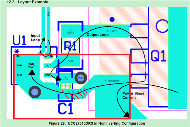
Fig.2
Best regards,
Hailiang
