This thread has been locked.

If you have a related question, please click the "Ask a related question" button in the top right corner. The newly created question will be automatically linked to this question.

UCC27517: Continuous enabled non-inverted (DBVR) input mode output reverse current sinks 500mA

Guru 54588 points
Part Number: UCC27517
Other Parts Discussed in Thread: UCC27714, UCC27516

Hello forum gurus,

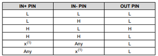
How can output sink 300mA continuous absolute maximum but also accept 500mA reverse, AKA negative current flow (Pg16,Fig.23)while the input is at CMOS low logic level?

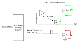
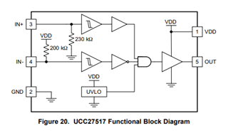
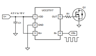
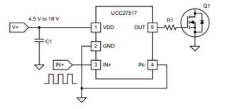
This UCC is used for existing brake drive circuit on PCB to replace competitions FL3100TSX. There is no way to disable output, shouldn't there be a pulse generator drive the output stages?  My concern is the NFET QG86nC requires more than 300mA continuous Roff gate drive where a series diode also boosts Goff current above Gon, in this scenario VDD=+15.2vdc.

I hope we can understand how it can work as 10 pieces are in the mail.

Thanks for ideas and help Slight smile

  • Hello,

    Thank you for reaching out!

    The UCC27517 can continuously sink/source up to 300mA of DC current according to the datasheet in section 8.1. The device can handle up to 500 mA of reverse current through the internal body diodes of the MOSFETs which offer low impedance to switching undershoot and overshoot transience. This undershoot and overshoot is not meant to be a continuous DC current. 

    Unfortunately, there is an error in figure 23 of the datasheet. This is a corrected figure figure posted above. As you can see in the new figure posted above, the Roh PMOS MOSFET is actually flipped from the original figure in the datasheet. The green body diodes in the figure helps sink to the overshoot transience that can occur if the output is at a higher voltage than VDD. The red body diode helps sink the undershoot transience that can occur if your output voltage is below GND. 

    Above you can see the truth table regarding the input and output stage. 

    A MOSFET should not require a large continuous gate current like the one you are mentioning above. Once the gate capacitance has been charged or discharged, very little current is needed to keep the gate in steady state.

    Hope this helps!

    Thank you,

    Kevin

  • Hi Kevin,

    My figure 23 looks the same as your posted one except for the diodes added to handle 500mA (transient reverse currents) during PWM switching events was left out. The wording of the last sentence seems to imply the Totem pole drives can handle 500mA sink currents. "The outputs of these drivers are designed to withstand 500-mA reverse current without either damage to the device or logic malfunction"

    The green body diodes in the figure helps sink to the overshoot transience that can occur if the output is at a higher voltage than VDD

    Adding turn off resistor plus series diode (100Ω GRoff) has very short time of 302mA sink, another 100Ω GRon=152mA source. The typical SW time 100Hz (25ms) 50% duty but actual periods can vary into seconds of intervals for braking, cooling, braking again. I may change Gtoff 120Ω since 300mA sink is the absolute maximum driving a resistive load. I am attempting to make the GPIO port switch closer to 20Khz rather than 100Hz best case.

    Oddly the PWM 20kHz load count interrupt handler is not producing 20kHz pulses in the GPIO port brake drive, with 8mA slew rate. The best times 100Hz 25ms on/off gate time is not going to be within safe operating area of 250vdc 61amp NFET driving a restive power load >B+. The brake drive input to output stays low until the voltage monitor reaches the on/off points 50% duty  

    We also use the UCC27714 with enable control so the added GR0ff resistors (51Ω) are only 49.9µs GRoff (409mA) sink while the PWM inputs drive switch states. Of-course these outputs switch inductive loads (HO/LO), both have hard pull downs during shut off to minimize switching reverse currents, no green/red diodes either Ho/Lo outputs.   

    For UCC27517 Psw was 3.288mW using 2 external resistors but the datasheet omits power dissipation via plastic case. Is the Fsw value (20Khz) to be in microseconds (0.000050) otherwise the resulting power value is huge? I also read SPRA953C–December 2003–Revised April 2016 to determine PD what a leap it takes from the old maximum PD method.

  • Hi,

    Thank you for reaching back out!

    Could you please send me a schematic of your design so I can have a better understanding of what's going on so I can better help?

    Looking forward to hearing back!

    Thank you,

    Kevin

  • Hi Kevin,

    You believe the output once switched low will not sink to the maximum current for very long. Seemingly still limits 4 amp sink to an unrealistic much lower QG/Nc current without use of enable control? Oddly section 9.3.4 makes a confusing statement "pulling down -IN to VDD disables the output when +IN is pulled to ground." How does -IN voltage ever get pulled down to VDD? Testing I use a jumbo LED on the output with anode facing RoL (150Ω). If the +IN Schmidt trigger only fires on the rising/falling edges (pulse generator) that could in effect be a control over the output sourcing >300mA on extended low times without an enable function. Can you verify if that is true or false? 

    9.3.4 Enable Function
    As mentioned earlier, an enable/disable function is easily implemented in the UCC27516 and UCC27517 using the unused input pin. When IN+ is pulled down to GND or IN- is pulled down to VDD, the output is disabled. Thus IN+ pin is used like an enable pin that is based on active-high logic, while IN- can be used like an enable pin that is based on active-low logic.

    Brake circuit has -IN tied to GND and only the +IN being switched. Seemingly the need for very short gate drive ON pulse-width (<35µs) as to minimize 300mA sink current during -IN (extended) low times. Datasheet text seems to neglect any mention the output 4amp sink/source may-not be achieved without an enable control as it will exceed 300mA absolute MAX during extended -IN low state times with higher QG/Nc drive strengths >300mA?

    BTW: UCC27714 level shifter has pulse generator but both LO/HO will not produce output pulses <100ns Pg.22 Fig.47. It may share similar design stages UCC27517?

    Regards,

  • Hi,

    I just accepted your friend request! When you get the chance private message me the schematic. I will get back to you soon with a response!

    Thank you,

    Kevin

  • Hi,

    Thank you for your patience!

    Regarding the enable functionality, below you can see that the the IN+ pin is pulled down to ground and the IN- pin is pulled up to VDD. This means that when the pins are left floating or unbiased, IN+ will be held low, and IN- will be held high. The correct verbiage is that IN- is pulled up rather than pulled down so apologies for the confusion there. In order to have enable functionality, IN- will use active low logic to enable the output of the driver.  With your current configuration of tying IN- to ground, the output will always be enabled.

    UCC27517 can sink/source up to 4A of current in all configurations types. The examples below are an inverting and non-inverting configuration of UCC27517. In these cases below all the datasheet specifications apply. You can sink and source up to 4A whether or not you use IN- as an enable pin.

    For UCC27517 Psw was 3.288mW using 2 external resistors but the datasheet omits power dissipation via plastic case. Is the Fsw value (20Khz) to be in microseconds (0.000050) otherwise the resulting power value is huge?

    Regarding the power dissipation formula, Fsw is to be used in Hertz, so in your case it would be 20000Hz.

    Hope this helps! If you have further questions please let me know!

    Thank you,

    Kevin

  • Hi Kevin,

    , Fsw is to be used in Hertz, so in your case it would be 20000Hz.

    Like I mentioned above an input 20000 produces an unrealistic huge dissipation value.

  • Hi,

    Thank you for reaching back out!

    Can you please show me how you calculated your switching losses? 

    Also please be aware that this device has a absolute maximum VDD rating of 20V. Its recommended operating range is between 4.5V and 18V. Based on the revisions in your schematic you would be breaking those rating.

    Thank you,

    Kevin 

  • Hi Kevin,

    I was multiplying 20000 for Fsw value, it's not 20Hz and instead used 0.000050 as Fsw since 20000 made PD =183,844mW. And using 20 for Fsw produced 181mW but even that seems much higher than original calculation (3.288mW) by multiplying Fsw 0.00005.  

  • Hi,

    Please check your private messages to see our calculation.

    Thank you,

    Kevin