This thread has been locked.

If you have a related question, please click the "Ask a related question" button in the top right corner. The newly created question will be automatically linked to this question.

TPS56339: Output voltage increase when load is connected

Part Number: TPS56339

Hello,

I have an observation in the behavior of the TPS56339 design. I have an input from an dc-dc 12V and stepping down to 3.3V using TPS56339.  This supply is given to an MCU daughter card to power the MCU.

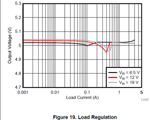
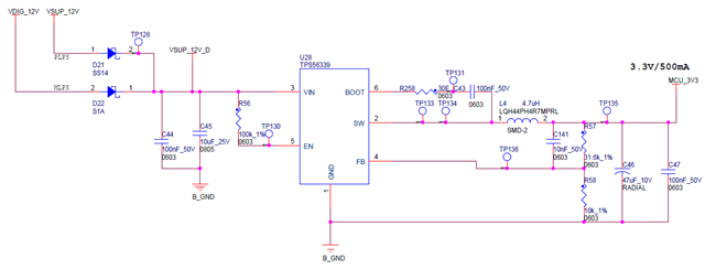
In the absence of MCU card, I see the output voltage is 3.33V. When I connect the MCU daughter card, the voltage increases to 3.421V. Below is the schematic for your reference.

Could you please let me know what could cause the voltage to increase.  Thanks in advance,

Regards,

Anand M

  • Hi Anand ,

    Normally the Vout voltage may change a little bit when loading changes because of loading regulation , while the change will be very small <0.1. You can refer below curve from datasheet.

    You may can use a E-load to check if it's related with load or not.

    If the loading isn't the reason for the voltage increase, pls help share more details about this issue .

    1. Which test point you are measuring --Vout? 

    2. What's the loading change ?

    3.Capture waveform of the "connecting " moment --VIN+VOUT+SW+Indcutor current in a single waveform , and provide some zoomin details.

    4. capture "3.33V" waveforms vs "3.421V" waveform --VIN+VOUT+SW+Indcutor 

    BRs,

    Young

  • Dear Young,

    I have captured the VOUT and SW waveform for you reference.

    Vout & SW - without load:

    Vout and SW with load:

    Is it the noise coupled on the output?

    I also noticed in the schematic that, EN is connect to Vin directly. But datasheet recommends EN to be <6V. I added a divider network on the EN pin and set the voltage to 3.6V. But still the problem persist.  Also providing the layout for your reference.

     ...      

    Let me know your thoughts on the same.

    Regards,

    Anand M

  • Hi Anand,

    Nice catch, the EN voltage should be <6V, you can add a resistor like you did or just remove the R56.

    The noise on the waveform seems large, pls make sure the output voltage was measured at the C46 with the closet loop, better with 20MHZ bandwidth to filter high freq noise.

    and it seems that device is working at light load even with loading , right ? Normally the output ripple in ECO mode would be larger than CCM mode because of the lower frequency . you can refer Figure 23 ~25 in datasheet. But it ripple seems too large. 

    and how do you measure the "3.33V" and "3.421V" ? by probe or multimeter ? 

    Regarding the layout , noticed that the BST trace was placed under IC, which is not recommended .

    Is there a GND layer not showed ? GND trace of IC is recommended to make it  as wider as possible

    Sorry that i can image more routing and placing with the 2 screenshots.

    BRs,

    Young 

  • Hi Young,

    Thanks for the immediate response. Yes I had "3.33V" and "3.421V" when measured with multi meter initially. When probed on scope, I got the short pulses on the output on the every switching pulse.

    Regarding layout, The device has solid ground plane under the IC.

    Shall I reroute the BST using jumper wire?

    How do I suppress  this behaviour in ligh load condition?

    Regards,

    Anand M

  • hi

     Yough will reply you next Monday.

    Shuai

  • Hi Anand,

    Sorry for the late reply.

    During  the debugging , you can try to reroute the BST trace to see if any improvement .

    About the light load behavior, you can check the Fsw and inductor current at the same time.

    If Fsw is  underlocking and inductor current valley touches zero, device works in eco-mode .

    If Fsw is same as CCM mode and inductor current valley touches zero, device works in DCM mode.

    others are in CCM mode. 

    ECO mode was set to boost the efficiency while it will bring larger output ripple.

    BRs,

    Young