This thread has been locked.

If you have a related question, please click the "Ask a related question" button in the top right corner. The newly created question will be automatically linked to this question.

BQ79656-Q1: Schematics for a base chip acting as a transceiver with no cells connected.

Part Number: BQ79656-Q1

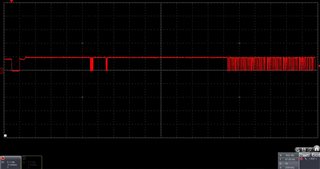
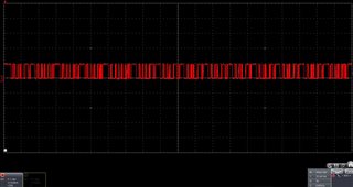
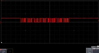
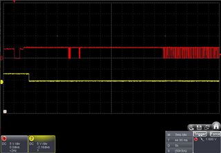
Hi all, We are still struggling to establish communications with the base chip in our stack. The base chip is serving the purpose of an isolated transceiver and thus has no cells connected to it at all. the chip is powered off of the PCB onboard 12v power supply. The chip wakes up as expected and all the LDO measure the correct voltages when awake; however, the fault line is immediately set and the chip sends no UART responses to any commands or requests. This is leading us to believe there is possibly some sort of layout issue which is causing the chip to fault on wake up. This is a custom PCB with an ATSAM3X8E host MCU and 3 BQ79656 chips where only 2 of them are connected to battery cells and the third base chip is just acting as a transceiver. I am attaching the schematics of the base chip in hopes that someone may be able to see an issue which would cause the chip to fault and shut down UART comms. Any other ideas would be helpful as well in trying to get communications established with the chip. Thank you in advance.

  • Hello Blakely,

    Sorry for the delay in response. I believe that this may be related to the RNPN (R1120, R1121) values on your PCB in combination with this low voltage supply. If you are supplying an external 12V, then I believe we should be using much lower values for RNPN. Can you try to replace these with 0ohms and see if you still have the issue? My expectation is that the voltage is high enough for transitioning to active mode, but not high enough to support the ~30mA needed for communications.

    If this doesn't help, it would be good to verify the waveforms on UART the RX/TX to make sure that the device is receiving correct commands.

  • I can provide pictures of the Rx line. This first picture is from power on.

    As you can see, we send the wakeup ping then there is ~22mS delay before we send first packet which the auto address sequence. Here is a zoomed in picture of that packet:

    This is what we send in that packet:

    Sending:  D0 03 4C 00 FC 24  
    Sending:  D0 03 09 01 0F 74  
    Sending:  D0 03 06 00 CB 44  
    Sending:  D0 03 08 02 4E E5  
    Sending:  90 00 03 08 01 D2 1D  
    Sending:  C0 03 43 00 FD 14  
    Sending:  C0 03 44 00 FF 24  
    Sending:  C0 03 45 00 FE B4  
    Sending:  C0 03 46 00 FE 44  
    Sending:  C0 03 47 00 FF D4  
    Sending:  C0 03 48 00 FA 24  
    Sending:  C0 03 49 00 FB B4  
    Sending:  C0 03 4A 00 FB 44  
    Sending:  D0 03 32 03 9D 85  

    Then a 4mS delay and a picture of the second packet:

    In this packet we send:

    Sending:  D0 00 17 40 36 E4  
    Sending:  C0 05 0C 01 E8 E5  
    Sending:  91 00 00 36 00 00 FC 94  
    Sending:  D1 03 31 FF FF 88 29  
    Sending:  D0 00 03 0A B8 13  
    Sending:  D0 00 07 02 BB 15  
    Sending:  D0 03 0D 0E 4D B0

    Then a delay of ~38mS we try to read module values sending:

    Sending:  C0 05 68 1F 42 2D

    We never see any response from the module. As soon as we release the Rx line to high after wakeup ping the nfault transitions from high to low.

  • Replacing the RNPN resistors with 0 ohm resulted in no change for me. Kyle has posted all of the waveform images as well. Hopefully this helps.

  • Also here is an image of the nfault line with th Rx line

  • Blakley and Kyle,

    These waveforms are a bit noisy, however I believe the device should be interpreting it correctly. Are you disabling the communication timeout (via the COMM_TIMEOUT_CONF register)? This is something we do in the GUI immediately after the autoaddressing procedure. Perhaps your device is timing out?