This thread has been locked.

If you have a related question, please click the "Ask a related question" button in the top right corner. The newly created question will be automatically linked to this question.

LM34936-Q1: Stability with light load at nominal and transition voltages

Part Number: LM34936-Q1
Other Parts Discussed in Thread: LM5176

I started with the LM5176 design spreadsheet and the  WEBench design: https://webench.ti.com/power-designer/switching-regulator/customize/18?noparams=0

I tried to include the schematic below but the quality of included images is very poor so if the link doesn't work then to recreate it in WEBench enter the design parameters minimum input voltage 12V, maximum 24V, Vout 18V and Iout up to 10A.

On reviewing the LM5176 design and WEbench design against the datasheet, Cslope was changed to 390pF, CC1 to 47nF and CC2 to 1500pF..

Because of part availability L1 is IHLP6767GZER4R7M01, M1 and M2 are SIDR626LEP-T1-RE3 and M3 and M4 are STL260N4F7

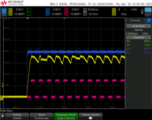
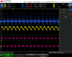
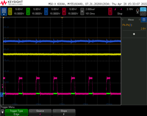
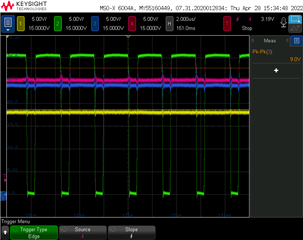
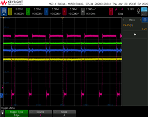
I have had four dev boards made and tested them all up to around 130W and have three main issues:

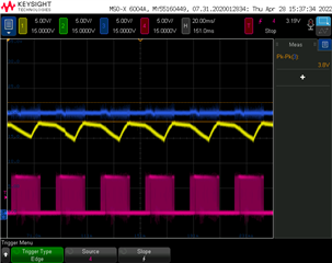
Firstly one of the boards does not start up at 12V unless it has a 2W load.

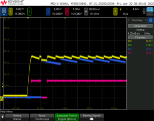
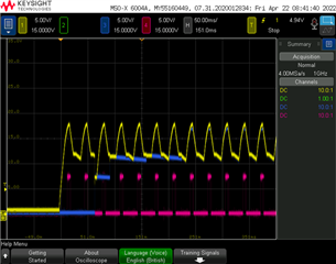
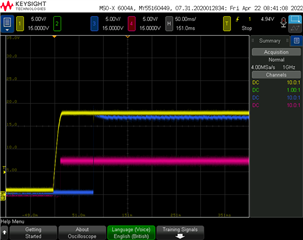
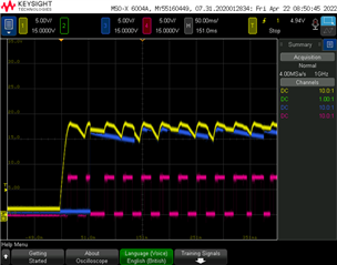
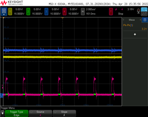
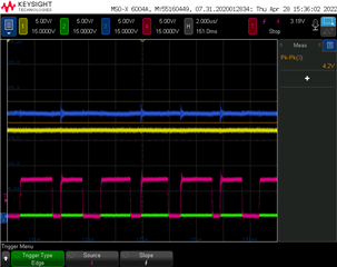
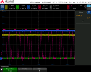
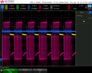
Secondly, all of the boards have instability between 17V input and 20.5V input unless they have a significant load, for example at 20V the stability only recovers with a 1A load (17.5W).

Thirdly, the overall efficiency is only around 93% at 100W with 24V in and 91% at 100W with 12V in compared to the design target of 98.3%.

So my questions are:

Can I make any changes to improve stability?

Can I make any changes to improve the overall efficiency?

  • As an update, I changed L1 from 4.7uH to 3.3uH to see if the lower DC resistance would improve the efficiency but it made no difference.

    It did however make a slight improvement to stability.  The PCB that previously required 2W to startup at 12V now starts up with no load and, although the 17V to 20.5V region still requires load to remove the instability the peak load required has now reduced from 850mA to 600mA.

  • As a further update, changed L1 to 2.2uH and reduced the switching frequency to around 250kHz (from 320kHz) but still no efficiency improvement.

    Once again though a significant stability improvement with almost the whole input range (10V to 30V) showing good stability at no load with a slight wobble at 19V where 200mA was enough to stabilize it.  So the whole boost range (10-18V) is stable and only the very first part of the buck range shows some slight load dependence.

  • Hi David,

    thank you for using the E2E forum.

    Unfortunately the provided link to Webench did not open the design but I could generate the design with your parameters.

    But based on past experience it would be good to share your schematic - to see exactly your setup. Otherwise a wrong assumption can easily consume a lot of time with seeking in the wrong direction.

    To check your design and also see the estimated losses you can also use the LM5176 Design Calculator: LM5176 data sheet, product information and support | TI.com

    This tool helps you to optimize the Compensation and check stability behavior on different load and supply points.

    This gives you more details and also show the contribution to the losses.

    The main contributor often are the FETs and selecting another FET (e.g. with higher R_DS,on and lower Gate Charge Q_G could change a lot.

    To further dig into your issue if the above suggestion do not help, it would be good if you can explain the seen behavior in more details and add a few scope shots.

    Best regards,

     Stefan

  • Thanks for the reply Stefan, as this is an open forum I am not able to post the schematic but I can confirm it is identical to the WEBench configuration with the exception of the component values in the initial post.  To expand on the detail of the performance I have added the testing of the board with the 12V startup issue, although as I stated above, this appears to be fixed by changing L1 to 3.3uH or 2.2uH.

    Check buck mode with no load.

     Apply 24V to VIN and VOUT should smoothly rise to 18V and PGOOD should go high.

     Tested OK with no load

     Check boost mode with no load

     Apply 12V to VIN - VOUT should rise smoothly to 18V and PGOOD should go high.

     Nothing should be hot.

     Regulation issue – yellow is VOUT, blue is the output of the charger circuit VBATT and red is PGOOD:

     PGOOD shows spikes at every peak point of VOUT.

     Later checks with electronic load and battery charging led to re-checking of this to see whether adding a small load would make it work.

     100mA (1.75W) load:


    125mA (2W) load:


    Check Buck/Boost and Boost/Buck Transitions

     Check that slowly increasing VIN from 17V to 19V has no effect on the VOUT output or PGOOD (i.e. it transitions smoothly from Boost to Buck).

     These checks were started at the lower voltage end with 125mA electronic load


    VIN (V)

    PGOOD

    Comments

    7.9

    OK

    Load 125mA. Cuts off below 7.9V

    8

    OK

    Load 125mA. Won’t startup below 8.6V

    10

    OK

    Load 125mA

    12

    OK

    Load125mA

    14

    Cyclic

    14.3V needs 150mA load

    16

    OK

    OK with no load

    17.1

    Cyclic

    Needs 125mA load

    18

    Cyclic

    Needs 600mA load

    18.5

    Cyclic

    Needs 750mA load

    20

    Cyclic

    Needs 850mA load

    22

    OK

    No load

    24

    OK

    No load

    26

    OK

    No load

    28

    OK

    No load

    30

    OK

    No load


    The 14.3V and 17-20V traces looked different to the initial 12V startup trace.


    Check that slowly decreasing VIN from 19V to 17V has no effect on the VOUT output or PGOOD (i.e. it transitions smoothly from Buck to Boost).

     Identical behaviour to the positive going performance, no appreciable hysteresis.

     Load current test in buck mode without battery

     Using the electronic load switching between 1A and 2A.

    VIN (V)

    LOAD (A)

    PSU Current (A)

    Load Voltage

    Efficiency (%)

    23.7

    8

    6.26

    17.36

    93.8

     Load current test in boost mode without battery

     Using the electronic load switching between 1A and 2A.


    VIN (V)

    LOAD (A)

    PSU Current (A)

    Load Voltage

    Efficiency (%)

    11.79

    4

    6.38

    17.56

    93.4

    11.73

    5

    8.00

    17.49

    93.2

  • Hi David,

    thanks for the details. Also understand that you can not share the full schematic.

    If the part of the LM5176 identical to what is shown in Webench cannot be extracted, can you try to generate the Webench link with this steps:

    Open your design

    Click on the 3 dots on the right

    Share design , public link, get link

    and paste this here.

    I would like to ensure I have the right configuration, e.g. Dither, Switching frequency, Hiccup mode, Slope

    What is CC1 and CC2 - it looks like this name do not match with Webench names.

    Best regards,

     Stefan

  • Hi Stefan

    I would normally share the schematic but I would have to clear it with the client first, alternatively I could send it to you direct as we have an NDA with TI.

    Here is the public link:

    https://webench.ti.com/appinfo/webench/scripts/SDP.cgi?ID=DC0023A67A4EA8B4

    I did add a dither capacitor (3.9nF) but this has been shorted out to avoid any possibility of affecting the performance.  Also, I initially had additional FET gate resistors but these have been replaced with wire links. All other parameters are as per the standard configuration.  CC1 is Ccomp and CC2 is Ccomp2.

    Interestingly, WEBench appears to have chosen slightly different values for Cslope, Ccomp and Ccomp2.  From my notes when I first ran WEBench it came up with 220pF, 15nF and 330pF but it is now saying 160pF, 10nF and 220pF.  When I went through the datasheet calculations I calculated values of 390pF for Cslope, 47nF for Ccomp and 1500pF for Ccomp2.

    My observations so far are:

    Reducing L1 from 4.7uH to 2.2uH seems to dramatically improve stability but may reduce efficiency.

    Increasing Rt from 23.2k to 33k (reduces switch frequency) does not seem to affect efficiency.

    Changing Cslope/Ccomp/Ccomp2 from 390pF/47nF/1500pF to 270pF/20nF/270pF does not seem to affect stability but may reduce efficiency.

    Although I am measuring efficiencies of around 91-94% at 100W, nothing is getting hot in the circuit so I am trying to figure out where the 6-9W is going.

    Best regards

    Dave

  • Hi Stefan

    I have managed to anonymise the schematic and attach it below as a pdf, please let me know if it works OK.  I tried to include it as a jpeg but it seems to be included at reduced resolution.  Note that the gate resistors R319, R320, R321 and R322 have been replaced with wire links as mentioned above and C302 is not fitted and R341 is fitted.

    Best regards

    Dave

    E2E_Buck_Boost_Schematic.pdf

  • Hi David,

    when clicking on my name you can connect with myself and then also send private messages.

    Another question: within Webench the capacitors on the outside are drawn only one time but marked with Qty=3 or 5.

    Have you added this capacitors with the given quantity.

    Best regards,

     Stefan

  • Thanks Stefan

    I saw the 3 off for the 33uF electrolytic capacitors, and put in 2 x 47uF but it looks like I must have missed the 5 off next to the 4.7uF ceramics.  Does this mean I need 70uF of ceramics?  I only have 20uF at the moment.

    Looking at the input side, I only have 47uF electrolytic and 10uF ceramic, I am not sure why as I calculated that I needed 94uFand WEbench says 122uF but all electrolytic.

    Would this affect the stability and/or the efficiency?  I did try adding 30uF ceramic on the input side but it didn't make any difference to stability, I didn't check efficiency.

    Best regards

    Dave

  • Hi David,

    the schematic is good as pdf.

    Can you share the Capacitor type you have used for C308/C309 and C310/C311.

    The might be an issue with the ESR and also would like to ensure that C310/C311 are electrolytic caps (as Ceramic caps would have the DC BIAS behavior).

    Thanks,

     Stefan

  • Hi Stefan

    C308/309 are X7R ceramics (MPN CL31B106KBHNNNE) and C310/C311 are electrolytic, automotive type EEE-1VA470WP.

    I just added 50uF of the X7R capacitors to the output and it didn't seem to affect the stability over the voltage range or the efficiency at 24 V (buck mode) but it seems to have made a big difference to the efficiency at 12V (boost) from 92.4% @ 76W load to 95.7%.

    Best regards

    Dave

  • Hi David,

    while reading through the information you provided a few more times and trying to understand the root cause of this behavior I have a few more questions:

    - can you probe the input voltage as well when in the error case. Is this stable as expected

    - for your scope plots you also show charger circuit VBATT - can you explain what that is and why this might be relevant to have it on the scope plot.

    The additional capacitor on the output did decrease the total ESR of the output cap. This helps (esp. for the Boost) mode to have a higher efficiency as the loss in the capacitor over the ESR is reduced. Therefore often multiple of the Capacitors put in parallel to reduce the ESR and keep the Current through the capacitors in the required / allowed range. Sometimes the rule of thumb with a Cap per 2A output current is used.

    Best regards,

     Stefan 

  • Hi Stefan

    Apologies for the confusion - I was monitoring VBATT for  other reasons, it is the battery input/charger output and only uses the buck boost circuit as the voltage source for the charger circuit so I monitor it when doing load tests involving charging.  

    For the efficiency figures I just test with an electronic load so the charger efficiency is not factored in.

    Here is a plot of VIN in blue, VOUT in yellow and PGOOD in red in the fault condition.

    You can see some noise there - here is an AC coupled plot with an expanded voltage range showing pk-pk of 3.65V around the 20V input.

    Best regards

    Dave

  • Hi Dave,

    I think you see here a lot of noise pickup with the measurement.

    You can try to use the so called tip-barrel measurement method and add the Bandwidth limit of the scope to make this measurement better.

    But still the 600mV is quite large, can you please try to add some more capacitor on the input side to get the supply more stable.

    Please also check the (combined) ESR of the input capacitors - having something in the range of 10mOhm or less would be good.

    It would also be good to see a picture with the gate drive signal (e.g. LDRV1 and LDRV2 - together with the output voltage and input voltage)

    Best regards,

     Stefan

  • Hi Stefan

    Here are some zoomed in traces of normal operation and the pulses are stable and don't change.

    VIN is Blue, VOUT is Yellow, LDRV1 is Red and LDRV2 is Green

    VIN is Blue, VOUT is Yellow, HDRV1 is Green and HDRV2 is Red (I mixed them up on this one, the rest have HDRV1 Red/HDRV Green)

    In the fault condition, the pulses are not stable, there are two zoomed in ones to show the range and a zoomed out one to show the overall picture.

    VIN is Blue, VOUT is Yellow, LDRV1 is Red and LDRV2 is Green

    The same for HDRV1 and HDRV2

    VIN is Blue, VOUT is Yellow, HDRV1 is Red and HDRV2 is Green

    Best regards

    Dave

  • Hi Dave,

    one of the scope plots show a changing duty cycle with smaller and wide pulses.

    This is typically a sign of an issue with the slope compensation. (I am not sure why this only should appear a very low load but would like to check on that).

    So can you change the capacitor for the slope compensation C303 to e.g. 180pF (maybe even go down to 150pF).

    Best regards, 

     Stefan

  • Hello Dave, 

    I have not seen an update on this thread for the last 7 days.

    Maybe you could solve this issue already in the meantime, in this case it would be great to press the is solved button.

    If there is still something open, just let me know with the new details.

    Best regards,

     Stefan