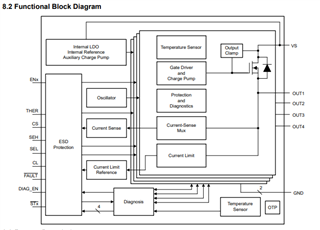
what internal topology below ICs having for driving the switch? Whether it is Solid state device (SSD) based or semiconductor-based design. We require this info to take as note for some test conditions.
This thread has been locked.
If you have a related question, please click the "Ask a related question" button in the top right corner. The newly created question will be automatically linked to this question.
what internal topology below ICs having for driving the switch? Whether it is Solid state device (SSD) based or semiconductor-based design. We require this info to take as note for some test conditions.
Hi Saranya,
We cannot share intricate details about our internals.
At this time, the most we can provide is what is available on the datasheets:
Each channel is driven individually with a gate driver circuit and a charge pump to push the NFET into the linear mode of operation to allow for low R_on and high current handling capability.
Thanks,
Shreyas