This thread has been locked.

If you have a related question, please click the "Ask a related question" button in the top right corner. The newly created question will be automatically linked to this question.

TPS63802: Device burns for unknown reason

Part Number: TPS63802

Hi Team,

Our customer designed a power supply using TPS63802DLAR based on the Webench simulation in the link below. 

webench.ti.com/.../153

However, he didn't find the original coil L1 TDK NLCV32T-R47M-PFR so used JSHC0520-R47M instead.

Sometimes the TPS63802 burns for no apparent reason. The maximum load current is not more than 120mA.

Our customer would like to know if the JSHC0520-R47M coil is suitable for this application. He also wants to confirm what could be the reason that the chip burned.

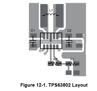
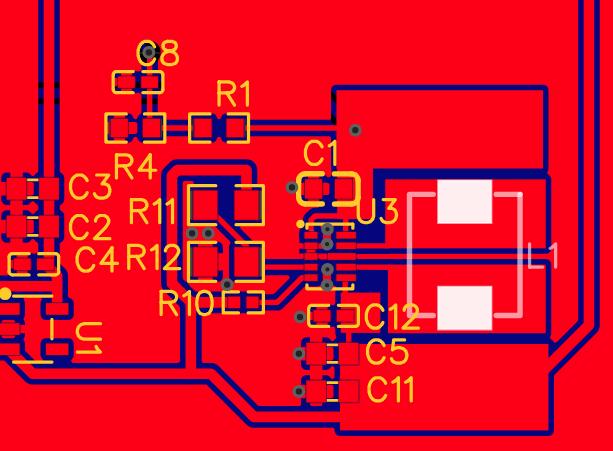
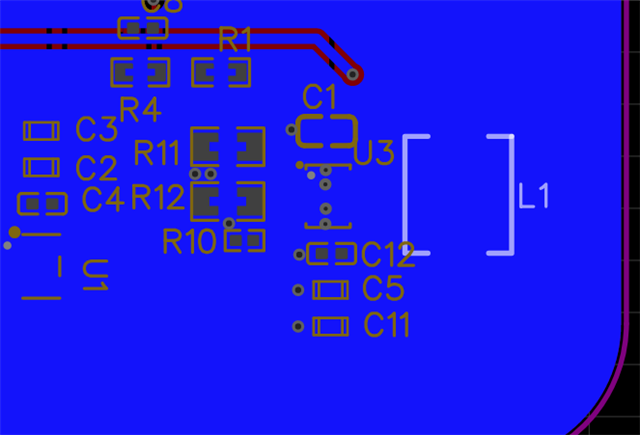
Here are the schematic diagram and PCB layout
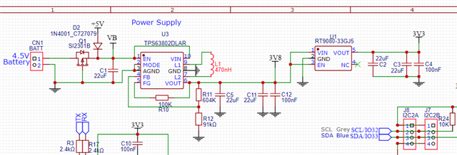
 Regards,

Danilo

  • Hi   Danilo,

    i think the inductor should not be the root cause.

    do you find any pins shorted to GND?  espicially Pin Vin L1 L2 Vout, could you help to check?

    Regards

    Tao

  • Hi Tao,

    According to our customer,

    Unfortunately the chips are so small I can't find them.

    I understand this is a problem, but can you tell me if the design of the PCB and the electrical circuit is correct?

    If another power supply burns, I'll save the chip.

    Regards,

    Danilo

  • Hi   Danilo,

    the schematic is ok and layout is not bad.

    input part has a good layout but it is voltage is high and output put has a not so good layout but the voltage is lower.

    i am not sure. but find which PINs shorted to GND is important to get the root cause. 

    once we get the PIN shorted, we can do some bench to confirm with same board but different devices.

    Regards

    Tao

  • Hi Tao,

    Here is the response of our customer.

    I found that I have a sort circuit of 3.3V in the periperal of the board,  This caused a current of 1.5A for a long time and this is probably what caused the chip to burn.

    1. Is it possible to set a current limitation in the supply to prevent such a case?

    2. Input part has a good layout but it is voltage is high and output put has a not so good layout but the voltage is lower.

    a. What do you mean you say “voltage is high”?

    b. And what can I improve on the output?

    Regards,

    Danilo

  • Hi   Danilo,

    1. Is it possible to set a current limitation in the supply to prevent such a case?

    device itself? no, it is impossible. it should be done with a complex external circuit. and i think it is unnecessary.

    2. Input part has a good layout but it is voltage is high and output put has a not so good layout but the voltage is lower.

    a. What do you mean you say “voltage is high”?

    the input voltage is 5 volt, right? i mean 5V is a high voltage for this device. 

    b. And what can I improve on the output?

    without re-design of layout, you can swap the location of C5 and C12, also during bench, i think you can connect the Gnd of output cap to Pin GND of device with a thick and short wire. it will help to find the root cause, i think the damaged device is caused by the parastic inductor.

    once we find the root cause. we can redesign the layout and make sure the parastic inductor of main power loop is as small as you can.

    the layout example in DS is really a good one.

    Regards

    Tao

  • Hi Tao,

    I just received this feedback from our customer.

    Thanks for the support.
    I change the PCB as you recommended, I hope it will solve the problem.
    Regards,
    Danilo
  • Hi   Danilo,

    Same hope from my side Grin

    Regards

    Tao