This thread has been locked.

If you have a related question, please click the "Ask a related question" button in the top right corner. The newly created question will be automatically linked to this question.

TPS542A52: Strange behaviour of the output

Part Number: TPS542A52

Hi,

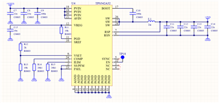
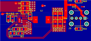
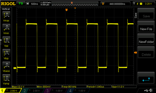
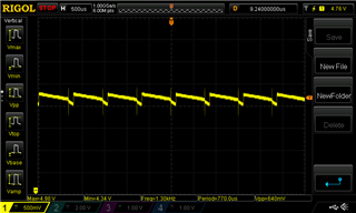
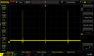
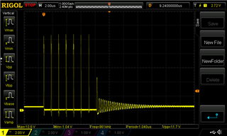
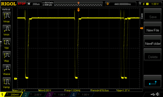
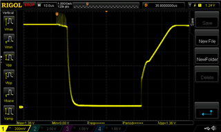
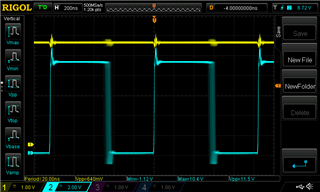
I designed PCB with TPS542A52 and it does not work properly. When power turns on, output goes to 5V but when we connect some load to it (like 100 mA) it immidiatelly goes down and after load is removed it does not recover to 5V again, only to ~0.4V. I have 3 PCBs and every behave the same way.
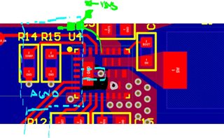
The strange thing is that i did exactly same schematic and layout before in other PCBs and it worked perfectly fine. It sounds like bad soldering but I also checked it. 
I tried to pull-up enable pin to some voltage (3.3V) to be sure that enable pin is above 1.2V threshold. Then output do not charge to 5V even without attached load - it stays at 0.4V.

So my question is: Do you know what could be a cause of this behaviour?

Best regards 
Tomasz

  • Can you share schematic and pcb layout?


  • Like I wrote before, I did the same schematic in other board at it worked perfectly fine.
    It is 2 layer PCB - blue layer is all ground.

  • If you power off and on with VIN, does the device regulate to 5V  with no load.   

    Can you use an oscilloscope to individually probe  VREG  (C15),   SREF (R12) and SW  at no load and 100mA. 

  • Yes, when I power off and on Vin, I have 5V output voltage with no load.

    I measured what you asked.

    1) When output is 5V and there is no load:

    VREG = 4,62V, it is DC signal, and there is nothing intresting, its behave the same like TPS542A52 working in my other project.

    SW = same situation, its working properly:


    SREF = when I attach probe to SREF the output goes low (~0.4V) - the same behaviour when I attach some load to the output

    2) When output is 0.4V (with load or when I try to measure SREF)

    VREG: 


    SW:


    zoomed: 

    SREF:


    zoomed:


    It sound like it is problem with 1.2V reference at SREF but I don't know why.

  • I can see that the VREG is changing voltage.   I would expect the VREG voltage to remain steady.   

    With VREG drooping, I think the device may be triggering the uvlo and cuasing a restart. 

    Did you probe the VIN voltage  (VSYS rail ) with no load and full load.   It is input voltage steady. 

  • The VREG voltage is changing only when output already does not work. Input rail is steady - with 9V input it is beetween 8.8V-9.2V. When output stop working it drops to 7,5V for short period of time so it does not trigger UVLO.

    I observed that I can load up to 400mA on this output without any problems but to achieve this I need increase load current very slow, like 10mA. When I try load more than 400mA the output goes down. 

    400mA load
    Blue - SW
    Yellow - 5V Output

    Like I said before the worst thing is that output stop working when I touch SREF with probe, so something there should be the problem but layout and components are good so I cannot figure it out.

  • SREF sets the voltage reference that the converter will regulate to the  VSET pin voltage x 5.   The 12kOhm on the

    SREF is greater than the 6kOhm limit which is in the inline with datasheet recommendation. 

    The device is behaving as though noise is coupling onto one of the internal signals causing the device to shutoff and restart.  

    The TPS542A52EVM has a 10 ohm resistor from PVIN to AVIN and a 0.47uF from AVIN to AGND.   

    On your layout the AGND pin 8 has a VIA near it and the nearest via that ties to PGND is closer to pin 29 than pin 25.

    The pins 29 to 33 is the source of the low side mosfet and there will be ground bounce when the power stage switches. 

    I suspect the combination not having the AVIN filter, the agnd via locations and the IC  and the loading of the 100mA is enough to cause a noise coupling event to trigger a restart. 

    The very slow application of the load and gradually increasing load supports the noise hypothesis. 

     Applying an oscilloscope probe to SREF could couple noise into the device. 

    Since this schematic and layout worked on the previous boards, have you installed an IC that has shown the behavior on a previous board to see if the behavior follows the device.   Or have you taken an IC off a previous board that has worked and installed on the latest boards. 

    Are the ICs on previous and current builds from the same lot trace code. 

  • I switched IC between old and new board and IC is ok - old PCB works in both cases and new PCB doesn't work in both cases. 
    When i said that the layout is the same I omitted fact that previous PCB is 4 layer and the new one is 2 layer. Since you claim that noise can couple into internal signals, I guess that 4 layer board with close ground plane underneath can handle that noise while 2 layer PCB with 1,6mm thickness cannot.
    If you don't have more ideas how to improve this board I will close this question and probably design 4 layer board :D
    Thank you for your help.

  • thanks for the sharing the information.   It helps me understand how susceptible the device can be. 

    There a couple of suggestions, if you are open to revising the board beyond your first pcb layout. 

      See the image (pardon my artwork)   on another layer of pcb add an AGND pour, via connect the ilim, comp, and VSET components to agnd.  

    Connect to the AGND to PGND under the device with a trace that is less wide and use one via and move this via closer to the agnd pad.     

    Move the second via to between the pgnd pads. 

    Add a cap and res to a   vsys to vdd and agnd. 

    I believe these changes would yield the full performance of the device.   

    Best Regards