This thread has been locked.

If you have a related question, please click the "Ask a related question" button in the top right corner. The newly created question will be automatically linked to this question.

TPS5432: Designing with TPS5432DDA

Part Number: TPS5432

Hi Team,
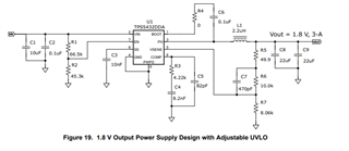
We are designing a buck converter using the IC TPS5432DDA.
The required output voltage is 1V.
The input voltage is from a Li-ion battery with a nominal voltage of 3.7V (2.8V to 4.2V).
Attached is the designed circuit.


The feedback resistors are a 10K resistor with a 470pF feed-forward capacitor and a 42.2K resistor to the ground.
I want to adjust the output voltage of the buck converter. So I am using the DAC of the processor to feed the VSENSE pin of the TPS5432DDA.
1). Is my calculations correct?.
2). Th output equation of the TPS5432DDA is given as 


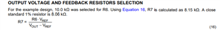
In equation 16 for the output voltage, the resistor R5 (49.9E) is not included. Why is that?.
I hope that resistor too has an effect on the output voltage.
Please correct me if I am wrong.


  • Hi Shibin,

    You need another resistor between the amplifier output and the VSENSE pin. Please see how to design this in the following links

    /cfs-file/__key/communityserver-discussions-components-files/196/1373.slyt777_5F00_Methods-of-output_2D00_voltage-adjustment-for-dcdc-converters.pdf

    http://www.ti.com/lit/zip/slvc780

    Please use the equation in the 1st link or the tool in the 2nd link to set the output voltage based on the low and high level from the amplifier/DAC output. Resistor R12 is usually inserted in the feedback path so that an ac voltage can be injected using a transformer for Bode plot measurements. You can also short it or replace it with a 0Ohm. In case you decide to keep it, there will be a very small error in the output voltage if it is not included in the calculations. In case you want a very accurate voltage, replace R15 in the equations with the (R15+R12).

    It is also recommended to check the phase margin of your system for the designed min/max VOUT using the TPS5432 PSPICE average model https://www.ti.com/lit/zip/slvm560. You can skip the amplifier/DAC and just modify R15 or R17 to set the min and max VOUT while doing this.

    Best regards,

    Varun

  • Hello Varun,
    Thank you for your reply.
    If I am not considering the Op amp and DAC, I hope a 10K resistor and a 42.2K resistor are the choices to generate a 1V output voltage. Please correct me if I am wrong.
    The lowest possible output voltage of the TPS5432DDA is 0.808V and the highest possible voltage is 4.5V. So do I really need to check the phase margin of the system?.
    Could you please explain the significance of checking the phase margin?.


  • Hi Shibin,

    Yes if you don't have the Opamp on the FB path, the 10K and 42.2K will give you 1V.

    If you will only operate at 1V, you just need to check the phase margin at 1V. Phase margin indicates how stable your system will be. A low phase margin can cause the output to oscillate. If you find a low (less than 45 degrees) phase margin while simulating the PSPICE average model, you will have to adjust the compensation network.

    Best regards,

    Varun

  • Hello Varun,
    Thank you for your quick reply.
    The IC TPS5432DDA is a buck converter that can generate from 0.808V to 4.5V.
    If that is the case why should I need to check the phase margin if I am operating the IC in the permitted working range?.
    Also, can I use WEBENCH to check the phase margin?.
     

  • Hi Shibin,

    Most of the buck converters are internally compensated for their output voltage range, recommended inductor & output capacitors and load. But the TPS5432 has external compensation that allows customers more flexibility. The compensation components in figure 19 of the datasheet is tailored for a VOUT of 1.8V. Since you have 1V in your application you will have to check if the same compensation network is sufficient to give you enough phase margin. The Webench model of this device doesn't have the option to check phase margin.

    Best regards,

    Varun

  • Hi Shibin,

    I checked the phase margin with the PSPICE model for your schematic. The compensation seems fine. The lowest phase margin I saw was 44 degrees when operating from 2.4 V Vin. All the other cases had higher phase margin.

    Best regards,

    Varun

  • Hi Varun.
    Thank you for your reply