This thread has been locked.

If you have a related question, please click the "Ask a related question" button in the top right corner. The newly created question will be automatically linked to this question.

LM27222: Device not switching.

Part Number: LM27222

Good Day,

I am using an LM27222 as two half bridges in a full bridge amplifier scenario.

As of right now I'm trying to diagnose a single half bridge.  I am using the sample circuit from the datasheet:

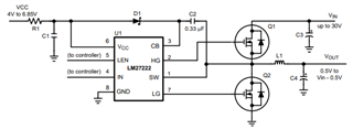
Where R1 is 1.5 OHM, C1 is 3.3uF.  Q1 and Q1 have a gate capacitance of 10nF and the bootstrap is 0.33uF.  According to common practice it seems acceptable to select a bootstrap capacitor that is greater than 10 times the gate capacitance of the FET and the input capacitance should be 10 times greater than the bootstrap capacitor.  Which the circuit meets.

I have a separate digital circuit that is the "controller" and the switching frequency at 20kHz at a duty cycle of 50%.  However, this burst of pulses occurs at a 10 percent duty cycle (The input to the amplifier is Low when this occurs).  I've also tried a standard 50% duty cycle at the same frequency and the LM27222 still does not switch as expected.

What other issues would cause the IC to not switch at the high and low side switch?  The bootstrap capacitor voltage at CB (Pin 3) referenced to ground, still seems to be too low (< 3V) and I'm not sure why this is as it seems as though there is plenty of capacitance.

Many Thanks,

Tyler

  • Hi Tyler,

    Thank you for posting on E2E. I will look into this further tomorrow and provide an update.

    Thanks,

    Daniel W

  • Hi Tyler, 

    Thank you for your question. Could you please clarify what is the VCC voltage you are using and the bootstrap diode PN to figure out the forward voltage drop?

    When switching, what is the voltage measured between CB and SW pins? For ease of the debug process, you can disconnect the output load and leave the Vin power off when measuring this. 

    Regards,

    Leslie

  • Hi Leslie,

    I am using 5V voltage and the bootstrap diode PN is SS14FL-TP.

    I don't see any switching located at the gate of the MOSFET's and the voltage at CB-SW is largely constant (With a few 100's of MV of oscillating as I assume it is trying to switch the FETS) I currently have no load.  I will confirm this measurement with a scope measurement today and report back later.

    When you say to remove Vin power do you mean only remove power from Pin 6 VIN and leave 5V at LEN and the bootstrap diode?

    I'm also going to dig into the layout further today and verify that there were no issues with board manufacture.

    Thanks,

    Tyler

  • Hi Tyler, 

    One question I forgot to ask yesterday: is LEN pin pulled high at all times? LEN pin enables the low side driver so it must be pulled high.

    When I mentioned not to power VIN, I meant the bus voltage (the voltage connected at the drain of the high side MOSFET). Basically, only have the gate driver operating by itself by powering VCC pin with 5V, providing 5V on LEN pin and then the PWM signal at IN pin. Then you can measure the CB-SW signal at the output and it should be at around 4.5V (VCC minus the diode voltage drop) and HG and LG should be switching. 

    If you still see issues it would be very helpful if you can capture the following 2 plots, preferably all 4 signals in the same scope plot, to help you debug further. For these measurements, please use tip and barrel method for signals referenced to GND, and differential probe for signals referenced to HS:

    • LEN-GND, IN-GND, HG-SW, LG-GND
    • VDD-GND, CB-SW, HG-SW, SW-GND

    Best regards,

    Leslie