This thread has been locked.

If you have a related question, please click the "Ask a related question" button in the top right corner. The newly created question will be automatically linked to this question.

LM5069: Circuit for Surge improvement

Part Number: LM5069
Other Parts Discussed in Thread: TPS2663

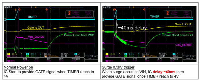
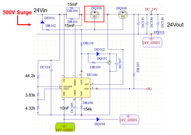
Customer would like to ask if the OUT pin of the LM5069 is connecting to VOUT rail ok? is there any side effect here? Or what else test you suggest to do with this configuration? Please see below plot for details. 

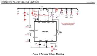
Since if customer following the topology on application report of the SNVA683, the recovery time (During OV protection Q1 and Q2 are turned OFF) is longer with several hundred ms and causing the system power/Flyback reset during surge event. Power reset is NOT allowed in servo drive application. 

After change the connection to VOUT, recovery time will become shorter about several ten mS, thus system/Flyback could not go into the shutdown with this configuration.  

Surge: 8/20uS with 500V on the 24Vin rail.

VIN: 24V

application: Servo Drive in Modeling machine

  • Hi Brian,

    If you are using device in power limit mode then you need to connect OUT pin to common source point otherwise it impacts Vds measurement.

    In case of dvdt startup method, you can connect OUT pin to Vout. But, I don't think it improves the OVP recovery. Can you share test waveforms Gate, Vout, timer and input current to understand 

    Best regards 

    Rakesh

  • pls see the waveform.

    Left side plot: Without surge test and in normal power on, the Gate driver starts to operate after TIMER pin is being charged to 4V.  

    Right side Plot: When surge testing, the Gate driver just starts to operate after TIMER pin is being change for 40mS. What happened?

    BTW, PG signals is NOT allowed to be pulled down to 0V during surge test. If PG signals is pulled down, the system power will be reset. Please check how to improve it. Thanks . 

  • Hi Brian,

    During surge event, the input swings towards negative and resets the LM5069. At the same time, D2 and R11 gives a path to discharge the residual charge on the GATE pin. From your waveforms, it looks these components are holding the GATE.

    What are the part# of DD101, DR102 in your schematic.? Is there bi-directional TVS diode at the input ?

    Can you remove DD101, DR102 and test once.

    Also, note the LM5069 does not provide class-A surge performance. The device resets and PG goes LOW during the surge event and hence you need to use large holdup capacitor for supporting the load. TPS2663 provides Class - A performance

    Best regards 

    Rakesh