This thread has been locked.

If you have a related question, please click the "Ask a related question" button in the top right corner. The newly created question will be automatically linked to this question.

UC2842: Feed back compensation of UC2842 for boost application

Part Number: UC2842
Other Parts Discussed in Thread: UC2901, UC2706,

Hi team,

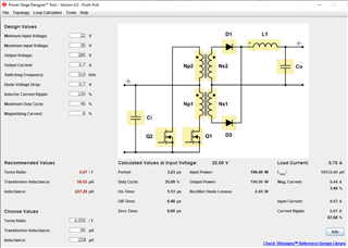
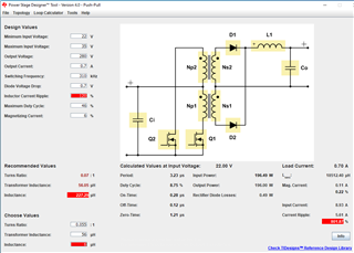
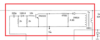
I am designing a DC DC Push-Pull converter with 22V to 34V input range, 280V output with 0.7A Load current. I have selected UC2842 as a PWM controller, UC2706 to convert single drive signal to two drive signal, and UC2901 as a isolation feedback controller. My transformer turns ratio is 1:18. 

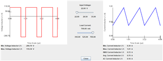
  1. I am able to achieve fixed 280V output with the input voltage variation from 22V to 34V but only under no load condition.
  2. My output voltage is not fixed it will vary +/- 15V to 20V under load condition, meaning my feedback compensation to UC2842 is not working properly. 
  3. I am facing an issue in feedback compensation at UC2842. How to tune feedback compensation values for UC2842 with respect to boost application?
  4. Is there any calculation sheet available for compensation tuning for UC2842 ?
  5. Is UC2842 will works for such a high transformer ratio application?

Thanks & regards,

Karthik Venkateshaiah.

  • Hello Karthik,

    I found your E2E post from a few days ago:  here.  To get a complete answer, it's very important to include schematics whenever possible.

    I examined your schematic and regulator specifications.  I think you have more than a simple feedback compensation issue.  The UC2842 is capable of satisfying your requirements, but you must use the correct power components.

    First, download and install Power Stage Designer from TI's web site:  Power Stage Designer.  Watch the training video.

    Using Power Stage Designer, I chose Push Pull topology and entered your specifications (Vin range, Vout, Iout, and Turns ratio).  I did not know your transformer inductance so I used the recommended value from Power Stage Designer (56uH).  Also, to start, I used the output inductance recommended by Power Stage Designer, 220uH.

    Notice the operating conditions:  Duty=35%, Input current (8.93A), Current ripple (0.61A), and On time (1.13us).

    Ripple current in the output inductor with 220uH output inductor is reasonable (see the blue waveform).

    Next, I changed the output inductance to the value from you schematic, 6uH.

    Notice the ripple current is extremely high now, 801%.

    The on time is extremely low (280ns) with 6uH output inductor.  It's extremely challenging to obtain such a low on time.

    The peak inductor current is 5.61A with 6uH output.  Can your magnetics/FETs handle this current?  This high current might explain your over-heating issue.  I suspect the entire PCB is getting hot, not just the UC2842.

    Lastly, I notice your question about not implementing the circuitry in the "red box".

    Did you leave out this entire circuit, including the current sense transformer?  The transformer creates a ramp (to the CS pin) so the UC2842 can perform PWM control.  I assume the transformer is included and you only left out the 2N2222 and it's 5 components.

    As for the transistor circuit, this is "leading edge blanking".  It is AC coupled from the gate drive waveform via 220pF.  The 2N2222 pulls low for a short time the moment the OUT signal rises.  This is required to have stable PWM operation.  It removes high-frequency current noise (ringing) when the FETs turn on.  Sometimes we use a small capacitor from CS pin to ground in place of the leading edge blanking circuit.

    I hope I have answered your questions and helped you get "back on track".

    Regards,

    Eric

  • Hi Eric,

    Thanks a lot for the detailed information. Thanks for making me to get back on the track.

    Thanks & regards,

    Karthik KV