This thread has been locked.

If you have a related question, please click the "Ask a related question" button in the top right corner. The newly created question will be automatically linked to this question.

TPS54428: Converter Damaged on Fast Transition of Vinput

Part Number: TPS54428
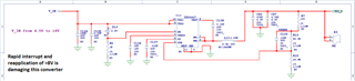
Other Parts Discussed in Thread: TPS54427,

Have approved either TPS54427 or TPS54428 for this application.  This circuit is working well for us for 5 years in production where the V_IN is a fixed 12VDC from another internal SMPS.  In that case D13 is 7.5V and R6 is 4.99K. 

Now, for a new design we want the external input range to be 4.5 to 18V, so we need to be enabled at a lower threshold and hence the change to D13.  R6 will rise to 10K to minimize power dissipation at Vin=18V.  Need to know how to protect this converter.

  • Hi Tim,

    1. Did device fail on TPS54427 or TPS54428?

    2. Did the device damage happen in power up or power down? Do you have waveform for EN and VIN during failure? 

    2. Did every board damage or just one board?

    3. What is load condition during failure?

    4. What do you want to protect with D13? Did you try to remove D13/R6 and connect VIN and EN together? Or just place a 19V zener from VIN to GND?

    Thanks,

    Nancy

  • Hi Tim,

    How did the device damage? Could you measure each pins? Which pins are damaged? 

    Thanks,

    Nancy

  • 1.  and 2b.  Seeing TPS54428 fail on 3 devices so far.   These boards are needed for a customer, so I'm quite hesitant to sacrifice any more.  It is possible to have them operate at 5V input or bypass the TPS5442x and operate from an external 3.3VDC.

    2a. In all 3 cases the device and downstream converters all worked as expected with initial abrupt power up at 6V input and with slow ramp up to at least 12VDC.  A subsequent abrupt power down and back up at 12V causes the 3.3V output to never come back.   I don't have a waveform but I will obtain one if I do any more sacrificial testing.

    3.  The load is an unprogrammed FPGA and subsequent 2.5V and 1.2V derived from the 3.3V output powering a Microchip MIC2230 dual buck converter.   Back driving the 3.3V from off board draws a load of 120mA and the 2.5V and 1.2V rails come up as expected.

    4.  The D13 and R6 combination on the enable are there to create an under voltage lock out at something less than the 4.5V minimum input.  I'd like to raise R6 to 10k ohms.

  • Pin 3 (VREG5) seems to be damaged.  An impedance meter to GND is showing 2 ohms on a damaged board but 600K on good board.  No significant difference on the other pins.

  • Hi Tim,

    The VREG5 is a LDO from Vin. This should be the line transient for a LDO circuit. The line transient response is function of the gain bandwidth of the LDO's control loop, step size and slew rate of input voltage changes. According to the application, reapplication of >8V with rapid interrupt, the step size and slew rate should be larger and damaged LDO.

    My suggestion: 1. You may change input cap C134 from 10uF to 22uF or larger to slow down Vin changing. 2. May change LDO output cap C136 from 1uF /16V to 2.2uF/16V. So the effective capacitance is still around 1uF to improve output variation.

    Hope this helps,

    Thanks,

    Nancy

  • On a newly assembled board, C134 input was changed to 20uF by adding a 2nd cap.  Likewise the C136 VREG5 cap was changed to 2uF.  This allowed successful power ONs at 12V, and 16V, but then that converter still failed permanently due to an abrupt connection to 18V input.

    Here is a view of the output and VREG5 startup from 12V input.  This looked the same at 15V and16V input.  But at 18V input the VREG5 never triggered the scope to obtain a sweep, meaning it never crossed above the trigger setting which was 0.76V.   This converter is now damaged like the previous samples with the VREG5 showing 3 ohms to GND.

  • Hi Tim,

    What is the slew rate on the VIN? I can check with design to see if there are any limitations on that. Other than that, for the latest tests, at 18V Vin, can you confirm if the VIN stays at 18V max or does it possibly exceed it? 

    Thanks,

    Amod

  • The test method was to remove, adjust as needed, and then insert the positive wire banana jack into a bench power supply at 18.0V.  So it could not surge above 18.0V but it does dump what energy the very large output caps inside the supply can feed though 18" of 14 gauge wire leads.  It would appear that this resulting input slew is still too high for the TPS54428.

  • Hi Tim,

    Thanks for the information. Is it possible to share the VIN waveform at the VIN pin of the IC? Just want to make sure there is no ringing which may exceed the abs max of the device. Also, the waveform will help ascertain the slew rate.

    Thanks,

    Amod