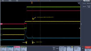
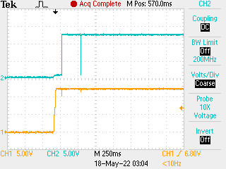
TIMER pin and GATE pin fall below ground as VIN drops below 6V when switching on large capacitive load - approx. 880uF. This event occurs approx. 250ms after the LM5069 switches on initial load of 22uF.
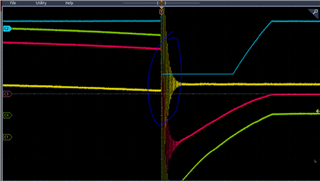
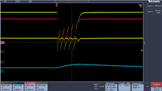
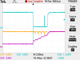
Scope1_zoomout.png and Scope2_zoomout.bmp provides an overview of timing. Scope1_zoomin4msres.png provides 4ms resolution of large capacitive load switching. Scope2_zoomin2msres.bmp provides 2.5ms resolution of large capacitive load switching - showing charging of actual load and LM5069 PGD pin.
Scope1_zoomin4usres.png provides 4us of large capacitive load switching. VIN pin drops below 6V triggering UVLO and POR thresholds. OUT and GATE pins drop >10V below GND. Timer pin drops >4V below GND. PGD drives low.
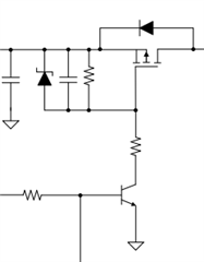
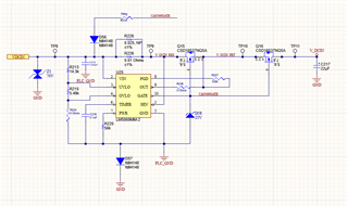
Protection circuit schematic.png includes the schematic. Design includes provisions detailed in TI SLVUAA1–September 2014 document.
Note that testing is conducted with a bench supply. The output of the supply is switched on and off - not hot plugging.
Please explain why GATE and Timer pins drop below GND and how do we prevent this. Note that the circuit eventually recovers and the capacitive load does come up.
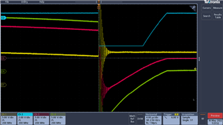
Scope1 legend:
Ch1 LM5069 VIN pin - 12V,
Ch2 LM5069 Timer pin
Ch3 LM5069 Out pin
Ch4 LM5069 Gate pin
Scope 2 legend:
Ch1 LM5069 VIN pin - 12V,
Ch2 LM5069 PGD pin
Ch3 LM5069 UUT V_MAIN