Other Parts Discussed in Thread: TPS1H200A-Q1, , CSD19537Q3, TPS2490, TPS2663, LM5069
Hi.
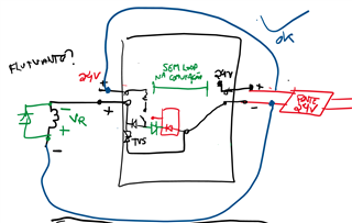
I am designing the new industrial data collector of the company, it will also have 2 protected transistor outputs / switches. The nominal system voltage is 24V, but we have seen in the history that some power supplies of the machinery have overvoltage, resuming we need to consider that the voltage of the power supplies can reach 36V, so I use 36V TVS diodes on all pins of the connectors, I mean 36V of reverse standoff voltage.
For the transistor outputs I had selected the smart load switch TPS1H200A-Q1 before, which the VCC maximum absolute is 42V, but after a while I started to think that this IC could be damaged easily by transients in this application.
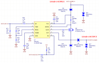
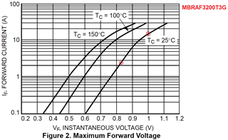
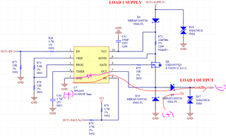
I searched so much in the internet for higher voltage load switches and did not found nothing enough. So I saw the hot swap controllers on TI website and found the TPS2491 interesting, because its ABS Max is 100V. The TVS diode used, SMAJ36CA, it can reach a maximum clamping voltage of 75V for a 8/20us pulse. The 2 series diodes of the schematic are rated for 3A continuous and 200V reverse voltage. The Mosfet N of the schematic is CSD19537Q3 and I chosed it because we already use it in another project.
Below are the calculations I did until now for the TPS2491.
---> Calculations of typical values only
Ilim Typ = 50mV / RS
Ilim Typ = 50mV / 22mR
Ilim Typ = 2.27A
2.27A ^2 * 0.022 = 113mW
Shunt = 22mR 1206 500mW or more
Vprog = Plim / (10 * Ilim)
Vprog = 60 / (10 * 2.27)
Vprog = 2.64V
VREF = 4V
Rdown = 2.64V, Rup = 1.36V
Relation = 2.64 / 1.36 = 1.941
Rup = 5.6K
Rdown = 5.6 * 1.941 = 10.86K
Rdown = 12K
---> Recalculating:
Vprog = VREF * Rdown / (Rdown + Rup)
Vprog = 4 * 12 / (12+5.6)
Vprog = 2.72V
Plim = Vprog * (10 * Ilim)
Plim = 2.72 * (10 * 2.27)
Plim = 61.7W
I Vref = 4V / (12K + 5.6K)
I Vref = 0.227mA
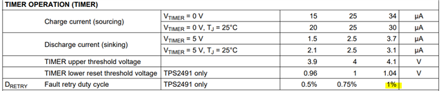
Ctimer = Tfault * 25uA / 4V
Tfault = Ctimer * 4V / 25uA
Tfault = 4.7uF * 4V / 25uA
Tfault = (4.7*10^-6) * 4 / (25*10^-6)
Tfault = 752ms
T re-enable ~= Tfault * 10
T re-enable ~= 7.5s
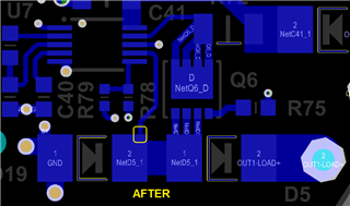
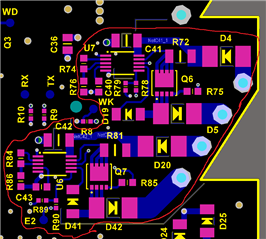
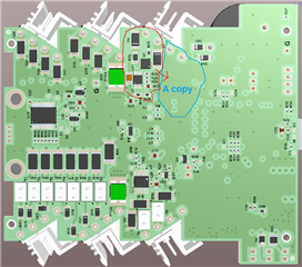
The PCB will have 2 times the circuit below, but I did it only one time until now, I want to check if it is all ok with it before copy this to a second identical circuit.
CURRENT SCHEMATIC:
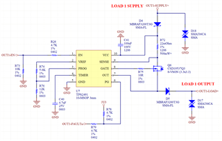
PDF OF THE SCHEMATIC:
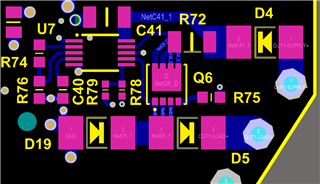
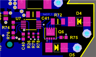
CURRENT PCB (2D):
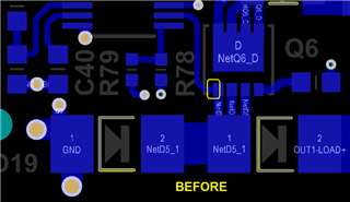
CURRENT PCB (3D):
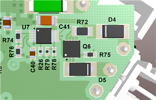
The board space is limited, it has 10cm x 9cm.
OBS: The 2 TVS diodes of 36V are placed at the other side of the PCB, very close to the connector.
OBSERVATIONS:
(1) Capacitor C41, 100nF, is Low ESL type.
(2) The circuit is intended to drive loads like relay coils, contactor coils, led strips, solenoids, self-oscillating buzzers. I know that these are the kinds of loads, but I don't have their specs.
(3) Lets suppose that the positive and negative wires of the power supply are directly connected to the input and output of the circuit, respectively, and the Mosfet is turned on, a short. In this case, the series diodes must not get damaged, what you can say about this? OBS: The series diodes withstand 100A non-repetitive peaks according to the datasheet.
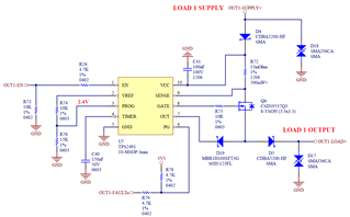
(4) For this circuit, it could be used another solution with some other IC of TI, like a load switch or something similar, but remember that the VCC ABS Max should be 80V or more, and that the IC should be small and the circuit also, you can have an idea of the available board space in the pictures.
(5) Would it be better to use TPS2490 instead? And in case of faults, the MCU monitor the PG pin? I wanted to know more about the operation of TPS2490... I imagine the following, please tell me if my reasoning is correct: for example, if Tfault is set to 1s through the capacitor on TIMER pin, then the MCU put level 1 on EN pin, the Mosfet conduces and if there is a short, the current would be limited and 1s after the switching ON of the Mosfet it will be turned off, and the PG pin will keep in level 0? (or will generate a pulse to 0?). Then the MCU put the EN pin to level 0, and after some time put the EN pin again to level 1, then the transistor will turn on again? It works like this? In TPS2490, is the signal of PG pin (going to low level) related to over-current and short circuit situations?
(6) Does TI engineers have observations or suggestions?
Thanks very much in advance,
Jeferson.