This thread has been locked.

If you have a related question, please click the "Ask a related question" button in the top right corner. The newly created question will be automatically linked to this question.

UCC28180: UCC28180 PMP8740

Part Number: UCC28180

Hi!
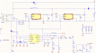
We are designing a charger board in which we added a UCC28180 chip for PFC boost conversion. we followed the circuit from the reference design of TI PMP8740 reference design | TI.com.

The schematics of our design are attached below. We are facing the issue that UCC28180  is not generating any pulses(PWM) to control MOSFETs, we are getting the same output voltage that is given on input.

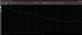
Moreover, We also tried to simulate the simulation example given on the TI website (https://www.ti.com/lit/zip/slum423) for UCC28180. but we are getting the same thing in the simulation results. we can not see any pulses on the gate pin and also output voltage trend is the same. 

we removed R19 (on VCC and Vsense pin) from the PCB to provide proper feedback up to 5V when 390 V is generated at the output of PFC. Please share your thoughts about this issue and suggest any solution. 

Thanks

  • Hi Dania,

    Thank you for your interest in the UCC28180.

    It appears you included R19 in your design based on J6 & R48 in the reference design. Those components were put in the design for a test purpose (although I don't know the specific purpose).  If the jumper on J6 was included, the PFC would not regulate (perhaps this was the designer's intent; to test the downstream circuitry without the PFC regulating).  So, you should not populate R19 and you can remove it from your design

    Regarding the simulation model, these are basically behavioral models, so the signal on the GATE pin (in particular) isn't what is actually seen on the GATE pin of the UCC28180. I know this can be confusing, but it makes the simulation times reasonable.

    I hope this answered your questions.

    Ray

  • Yes, I understand that thing but as I mentioned above, we removed R19 from our design. but still, we cannot see any output from the chip. But we have C16 missing on the PCB. Do you think it can affect our design? From the datasheet, we have seen that this set the gain of the error. unfortunately, we can have only 1uF and 10uF capacitors to put on C16. what do you think about which value we need to use if this capacitor is mandatory. 
    Thank you very much.

  • Hi Dania,

    I apologize as it sounded as though you were regulating once R48 was removed.  Start by adding C16 to close your voltage loop. Between 1uF and 10uF, I would suggest the 10uF. I would also suggest you change R9 to ~13kΩ.

    If you still don't get 390V on the output, please provide scope waveforms during startup (or just before and after the VGATE stops). I would need to see VCOMP, IL1 VGATE & VOUT

    Regards,

    Ray

  • I have connected 10uF at C16, 13K at R9 and removed R19. 

    Now I am not getting output similar to input.

    there are not pulses on the gate,

    I am getting 0.85V to 0.9V on VSENSE pin. 

    0.8 or 1 mV on VCOMP pin

    I can read from datasheet that if voltage at VSENSE reaches to 0.82V, device operation started and it got standby mode if voltage is less than 0.82V. 

  • Hi Dania,

    Yes, if there are no pulses on the gate, you will get approximately the input voltage on the output (due to peak regulation).

    I'm look forward to seeing the requested waveforms. Instead of VOUT, you can show VSENSE.

    Please also provide your input voltage range and output power.

    Regards,

    Ray