This thread has been locked.

If you have a related question, please click the "Ask a related question" button in the top right corner. The newly created question will be automatically linked to this question.

LM25011: Issue when attempting to use alternative LM25011A.

Part Number: LM25011

Hi,

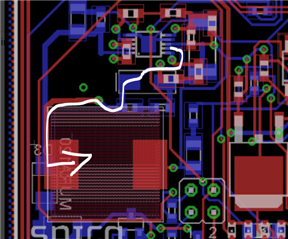
due to supply shortages we are considering replacing the LM25011 with LM25011A in our buck converter circuit shown below.

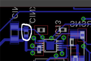
The test was semi-successful. Output voltage seems OK and stable both at minimum and max load. Frequency roughly the same. However, the voltage on SW pin worries me. With LM25011, the SW pin waveform is a nice square signal, as expected. With the LM25011A, there are sometimes two pulses without any off time in between followed by a short period of instability. See the following image in which red trace shows the waveform on SW pin and blue one voltage across Rsns.

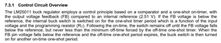
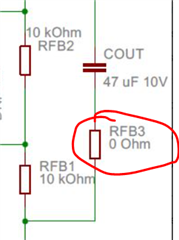
I've tried increasing RFB3 (R1 in chip's datasheet) to 1 Ohm, which should roughly equate to an increase in ripple voltage on FB pin by 100 mV. But it did not help.
With increased load, the waveform stabilizes on a normal square wave again within a few seconds.

Can anyone perhaps offer an explanation of what is happening on the SW pin, is it something to worry about and if so, how to stabilize the voltage seen there?

Thank you in advance for your help.

Converter parameters:
Vout: 5 V
Vin min: 12 V
Vin max: 24 V
Iout min: 0,12 A
Iout max: 2 A
F: 500 kHz

  • Hi Nejc,

    I believe you might be able to solve this problem by either slightly increasing the switching frequency or adding an additional minimum load. The difference between the 2 devices is that the A-version has a slightly lower minimum-off-time than the regular version, so that might explain the rapid back-to-back pulses.

    Could you also share the inductor current?

    Thanks,

    Andrew

  • Hello Andrew,

    first of all, thank you very much for your feedback.

    I'm not sure I understand how a lower off-time comes into play. Since the original IC (LM25011) has a higher minimum off-time than LM25011A it stands to reason that the circuit in question satisfies the minimum off-time requirement for both ICs. LM25011 as well as LM25011A. Does it not? Can you please help me understand this?

    I do not have a current probe but I used a 1 Ohm resistor in series with the inductor on its output side and got the following trace when measuring voltage across it (normal load on output):

    It seems to me that operation moved to discontinuous mode. Still... is the voltage on SW pin shown in my original post normal for discontinuous mode of operation of LM25011A?

    Here is the voltage over 1 Ohm resistor in series with L when load is increased and the voltage on SW pin below:

    I'm afraid I don't have the option to increase minimum load without PCM modification.
    I will get to increasing the frequency tomorrow to see if that helps and how much exactly I have to increase it.

    Am I correct in assuming I am targeting continuous mode of operation (Il never reaches 0) with SW pin switching in a more or less stable frequency without back-to-back pulses? And all of this for minimal as well as max load?

    Thank you.

    Nejc

  • Hi Nejc

    Let's see what happens when you change the Fsw (you might also need to change the L value).

    Also could you share your layout?

    Thanks,

    Andrew

  • Hi Andrew,

    I'm afraid I posted the wrong circuit in my original post. Below is the correct one. It's not that different but still.

    Today I've proceeded to increase switching frequency by changing the value of RT to 130 kOhm (according to my calculations this should give a sqitching frequency around 900 kHz). It unfortunately did not stabilize the SW pin. Below image shows how the voltage on that pin looks like after this change (top/blue trace is SW pin on original circuit using LM25011; bottom/red trace is with LM25011A, RFB3 1 Ohm and RT 130kOhm):

    And here's the image of inductor current (red trace):

    I've also tried increasing L to 33 uH. Below are images showing a trace from SW pin and the inductor current.

    It seems to me the larger inductor removed the oscillations. However the SW waveform still doesn't look right. I'd expect something like the blue trace in the second image of this post.

    Do you have a thought as to what those oscillations on the SW pin are? Is it the internal switch not being able to pull the pin to Vin perhaps? Or is the switch turned off during that time and the oscillation comes from the inductor?

    Do you have any comments to SW pin with 33uH inductor? Why the long off times and then 3 consecutive pulses?

    Any other ideas what to try?

    Below are some layout images you asked for.

    Thank you so much for your input!

    Nejc

  • Hi Nejc,

    Is this the switch node? This seems a bit large especially if it's spanning multiple layers. It could be picking up some noise. I would prefer the path from the IC to the inductor doesn't use any vias or long traces. The noise you are observing could be the large switch node picking up noise from elsewhere on the PCB.

    Also, we recommend placing the high frequency bypass capacitor as close as possible to the IC to minimize noise problems. 

    Thanks,

    Andrew

  • Hello Andrew,

    you have correctly identified the trace going from the SW pin to the inductor. Thank you the two pieces of advice. I don't have the option to modify the layout at this point. However, I've tried connecting the SW pin and inductor using a thick wire, soldering another filtering/bypass capacitor directly onto the LM25011A IC's pins and disconnecting everything else on the PCB to eliminate other noise sources. I'm afraid there were no changes. So while this may be beneficial for other reasons, the two suggestions unfortunately don't seem to help in solving this particular problem.

    Here are some other things I've tried today:

    • Replaced RFB4 with 0 Ohm.
    • Changed RFB1 and RFB2 values to 2 kOhm (wanted to go with 5 or 4.7 but didn't have them available).
    • Added a 470 nF at location CBST2.
    • Removed CBST1

    Some of those changes helped reduce the oscillations somewhat, but not completely. Also, back-to-back triggering of SW pulses remained.
    Still, output voltage was at the correct voltage and stable for all changes.

    Two questions keep rolling around in my mind:

    1. Is "double triggering", i.e., back-to-back pulses an issue at all? Could that be encountered also during normal operation?
      My take on this is that if the output voltage did not rise sufficiently after the first pulse, another one is needed. And possibly another and another until the output voltage gets back to the desired level. Note that the off time in-between the two pulses is roughly 80 ns, which is close to the specified minimum off time of 75 ns for LM25011A.
      It is unusual though, that the LM25011 does not experience this.
    2. In which scenarios can SW pin produce oscillations? The ICs internal logic should either trigger a fixed on-time pulse, or stay off. As I understand the IC's internal structure it does not have the option to generate a sine signal on the SW pin. So what are the scenarios in which that could happen?

    Any thoughts, comments and/or explanations for the two questions would be greatly appreciated.

    Thank you.

    Nejc

  • Hi Nejc,

    As far as I can tell, it could be that the reference voltage isn't meeting the threshold (or dropping below it slightly during the minimum off time) so the device powers another one-shot on time period. I believe it's functioning as the DS states:

    That's actually why I wanted to see if changed the frequency would have any effect. If you switch at a higher rate, then the reference voltage *should* be hitting that 2.51V limit more often before falling. But it actually had the opposite effect where the device is firing more pulses before staying off for some time.

    Could you check if there any shenanigans happening on the FB node? That might be the root of this issue.

    Thanks,

    Andrew

  • To add on, a colleague of mine also recommended that you could increase this series resistor with the output capacitor, so there's more ripple injection.

  • Hello Andrew,

    thank you for your suggestions. It looks like increasing ripple is indeed the way to solve this. By placing a 100mOhm resistor at position RFB3 and a 1nF capacitor at position CBST2, multiple triggering is eliminated. It appears though that selecting the right values is crucial. In my first post I mentioned that I used a 1 Ohm resistor at position RFB3 to see if the increased ripple resulting from that change would help. Unfortunately it didn't. I've also added 47 nF at position CBST2 during our troubleshooting in previous posts. Still, multiple triggering could be observed. Granted that somewhere in-between I've also increased L to 33 uH. 

    Anyway... I've then turned to a local circuit designer for help and he ended up with 100mOhm for RFB3 and 1nF for CBST2 as the values which solve the multiple triggering issue.

    As for the oscillations, those are normal for transition from continuous to discontinuous mode. And our circuit with LM25011A seems to operate at the border between the two modes during normal load (which is also the circuit's minimum load). With LM25011 the converter is obviously a bit further away from discontinuous mode. Not much though.

    If you have any explanation as to why my values for RFB3 and CBST2 (1 Ohm and 47 nF) didn't help while values of 100 mOhm and 1 nF do, I would be interested to hear your thoughts.

    Thank you for all your input and your help. Please also give my thanks to your colleague.

    Nejc

  • Hi Nejc,

    It actually makes sense why the device works better with the lower resistor and capacitor values as it actually will perform better with more ripple injection. That's my thoughts on it anyway.

    Thanks,

    Andrew

  • Hi Nejc,

    I haven't heard from you in a while.

    I'm going to assume this issue is resolved.

    Thanks,

    Andrew

  • Hi Andrew,

    sorry. I thought I accepted the answer and thereby closed this thread.

    Indeed, the issue is resolved. My last post explains how.

    Thank you again for your help.

    Nejc