This thread has been locked.

If you have a related question, please click the "Ask a related question" button in the top right corner. The newly created question will be automatically linked to this question.

UCD9090-Q1: Are there any reference design for UCD90XXX

Part Number: UCD9090-Q1
Other Parts Discussed in Thread: UCD9090

Hi, I'm now working on UCD90XXX series chips for Xilinx FPGA power sequencing.

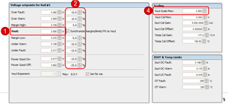
I have read the datasheet of ucd9090-q1、"Fusion Digital Power Designer GUI 7.0 for the UCD90xxx Sequencer User's Guide".

But  I still have a lot of doubts when I use TI‘s tools to design real project.

for example ,I don't have enough information to match the "title“ in below image to the real hardware pins.

Are there any reference design,which can help me to slove this problem.

Thx!

  • Hi

    The title is the function of the IO. please refer the attached quick guide.

    2133.UCD90xxx 简易使用手冊.pptx

    Regards

    Yihe

  • Hi yihe

    Thanks for ur reply,  it is useful to solve my doubts.

    There's  a new question after I read the attachment your given.

    In step 1, we input the voltage  which will be monitored. It is the real voltage value after voltage divider circuit.

    Why shoud we provide the  voltage divider informations in step 4, again?

  • Hi

    We recommend the voltage before divider. if you put the voltage after the divider, then the scale shall be set to 1 instead of real ratio.

    UCD9090 can only monitor up to 2.5V voltage, so for any voltage larger than this value, a external voltage divider is required so that a proper value can be monitored. Having the step4(scaling ratio) can allow customer to input the voltage before the divider at the step 1.

    Regards

    Yihe