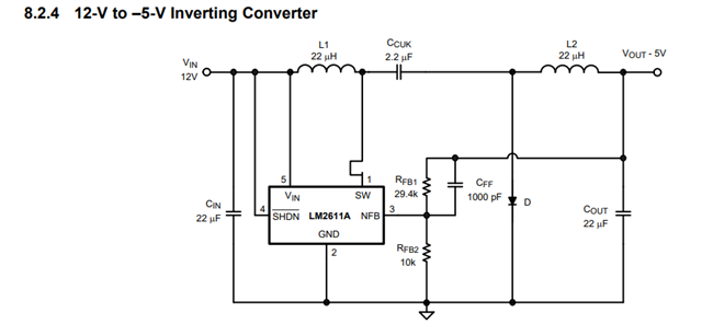
Hi Team
Customer spec is 12V to -12V@0.12A
1. Could you check that we can follow following design? Or what parameters need to be changed ?THX

This thread has been locked.
If you have a related question, please click the "Ask a related question" button in the top right corner. The newly created question will be automatically linked to this question.
Hi Team
Customer spec is 12V to -12V@0.12A
1. Could you check that we can follow following design? Or what parameters need to be changed ?THX

Hello Kygo,
Thanks for reaching out to us.
The example in Section 8.2.4 of the datasheet shows a conversion from +12V IN to -5V OUT.
To set a different output voltage, adjust RFB2 as per this formula:
VOUT * Rfb2 / (Rfb1 + Rfb2) = -1.23V.
To adjust the output voltage, we usually change Rfb2 and leave Rfb1 untouched, because changing Rfb2 will not affect the loop gain, and hence the stability.
To get -12V out, you may select a resistor of about 3.3K for Rfb2.
As the 12V input voltage is getting close to the maximum supply voltage of 14V, I would also want to mention section 9 of the datasheet:
The power supply must never exceed the absolute maximum rating of the device given in Absolute Maximum Ratings.
If the regulator is connected to the input supply through long wires or PCB traces, special care is required to achieve good performance.
The parasitic inductance and resistance of the input cables can have an adverse effect on the operation of the regulator.
The parasitic inductance, in combination with the low ESR ceramic input capacitors, can form an under-damped resonant circuit.
This circuit may cause overvoltage transients at the VIN pin, each time the input supply is cycled on and off.
This is why the datasheet also shows how to use a separate, lower (Biasing-)voltage for Vin, e.g. in Figure 31.
Best regards,
Harry