This thread has been locked.

If you have a related question, please click the "Ask a related question" button in the top right corner. The newly created question will be automatically linked to this question.

TPS7H4010-SEP: Reverse current blocking / load disconnect when Vin = 0V and Vout = 3.3V

Part Number: TPS7H4010-SEP
Other Parts Discussed in Thread: TPS7H2201-SP

Hi

I have a space application where the TPS7H4010-SEP looks like a good fit as a bucking regulator to convert +5VDC to +3.3VDC at 1.5A.

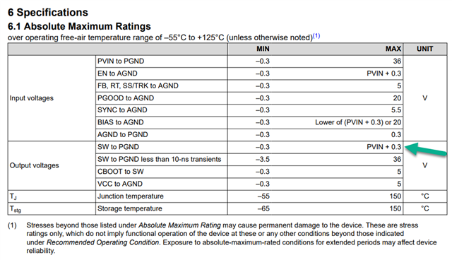
However, this input to this supply is sometimes unpowered while a second supply powers the +3.3V bus (Vin = 0V, Vout = +3.3V).  There is a design requirement that under those conditions, the supply blocks current flow from Vout to Vin.

Will the TPS7H4010-SEP block current flow from Vout to Vin when Vout = +3.3V and Vin = 0V?

If it does not block current flow, does TI have any low power dissipative recommended methods to add this feature to the supply?

Sincerely,

Doug Young

  • Hi Doug,

    My understanding is that no current will flow with VIN=0V even if the output is back biased to 3.3V, although I have never tested this mode before.  Also, I think utilizing the UVLO on the EN pin will force the device into a disable mode so that no current can flow through the power FET.  This is something that can be verified easily on an EVM which are available from the product folder on ti.com.

    Thanks,

    Christian

  • Hi Christian,

    Thanks for the response, I have a couple of follow up question / comments:

    -Is the pass FET inside of the TPS7H4010-SEP constructed in such a way that it will block back biased current flow, such as not having the intrinsic body diode or a back-to-back FET configuration?

    - FYI, I did run a PSPICE simulation using the TPS7H4010-SEP_trans model supplied by TI and it did allow for back biased current flow when Vout = 3.3V and Vin = 0V.

    - Is the UVLO / EN pin functional when the IC is not powered?  I've seen other parts in the past that required a minimum input voltage to maintain that functionality.

    Sincerely,

    Doug Young

  • Hi Doug,

    I will look into your questions and reply to you on Monday.

    Thanks,

    Christian

  • Hi Doug,

    The datasheet states the device is capable of starting up into a pre-biased output condition but does not explicitly state the condition on the input. I would guess biased input is assumed but don't know for certain.

    "TPS7H4010-SEP is operating in diode emulation mode during start-up regardless of mode setting. The device
    is capable of starting up into pre-biased output conditions. During start-up, the device sets the minimum inductor
    current to zero to avoid back charging the input capacitors."

    I will try to test an EVM if I have one available to see what current, if any, flows under this condition.

    Thanks

    Christian

  • Hi Doug,

    I confirmed there is reverse current from VOUT to PVIN when PVIN=0V and VOUT=3.3V.  The backbias comment in the datasheet refers to scenario when PVIN is applied, EN is low, and the output is biased from some other source.  

    Can you implement a load switch to isolate the TPS7H4010-SEP from the other 3.3V rail generator?  We offer the TPS7H2201-SP load switch.

    thanks

    Christian

  • Hi Christian,

    Thank you for running that test, it gives me a direction to follow on this design.

    Were you able to also verify that there is no back bias current when PVIN > UVLO, EN = 0 and VOUT = +3.3V?

    The idea of a load switch is a good one but the TPS7H2201-SP comes at quite a cost in terms of board space and dollars.  Does TI offer any plastic packaged radiation tolerant load switches?  If not, do you have application notes on isolating the output of the TPS7H2201-SP? 

    I am thinking of using back-to-back p-channel FETS that would be enabled when the TPS7H2201-SP is powered but if there is a more elegant solution I'd be will to consider using it.

    Sincerely,

    Doug Young

  • Hi Doug,

    Just to confirm, there IS back bias current when PVIN=0V and VOUT=3.3V.  I will check to see if this is still the case when PVIN is biased above UVLO but EN is held low.  This should not have any back bias current as I consider this is a typical operating condition.

    Regarding isolation of the 2201-SP, and other 'elegant' solutions, I will discuss with my colleagues who support the switches and get back to you soon.

    Thanks

    Christian

  • Hi Christian, the absolute maximum ratings for the output of this buck indicates VOUT can't be more than 0.3V higher than VIN. Wouldn't this be violated for the use-case given (PVIN=0, VOUT=3.3V)? Is this not a concern? Or is this value derived from from the body diode forward voltage of the high-side MOSFET so it wouldn't be violated in this situation?


  • Hi John,

    You are absolutely correct- the scenario would violate this abs max specification.  For some of our QMLV converters this restriction is not in the abs max table and reverse current is not a reliability concern.  But for this device, it seems it is. Therefore, you would need to isolate the output from the other source until PVIN is brought high. 

    Regarding a load switch, I will have our marketing team contact you directly via email to discuss space plastic load switches that might interest you.

    Thanks

    Christian

  • Hi Christian, I would be interested in the plastic load switches as well. We have an application with limited board space so a smaller solution would be helpful.

  • HI Dan,

    I asked our marketing team to contact you directly via email but I assume this hasn't happened yet.  I will inform them again so they can discuss plastic load switch solution with you.

    Thanks

    Christian