Other Parts Discussed in Thread: TPS63070, , TPS3840, TPS37
I have two questions. Here's the background of the circuit I'm trying to produce.
I'm trying to make a 5V power supply, powered by 4x AA batteries, using the TPS63070 buck-boost. I want the output to shut off once the battery voltage starts to collapse to avoid boot-loops, so I used a TPS3840PL25 to pull the EN line on the TPS63070 low, and latch it off with the circuit described in this note: https://www.ti.com/lit/an/snva836a/snva836a.pdf
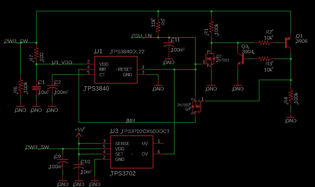
This works great according to my tests. However, I would also like to add a supervisor IC on the 5V output to protect the system downstream, mostly from output overvoltage conditions. I was trying to think of the best way to achieve this with the setup I have, and determined adding a TPS3702 to monitor the 5V line, allowing it to latch the EN pin on the TPS63070 off in an error state, was a good option.
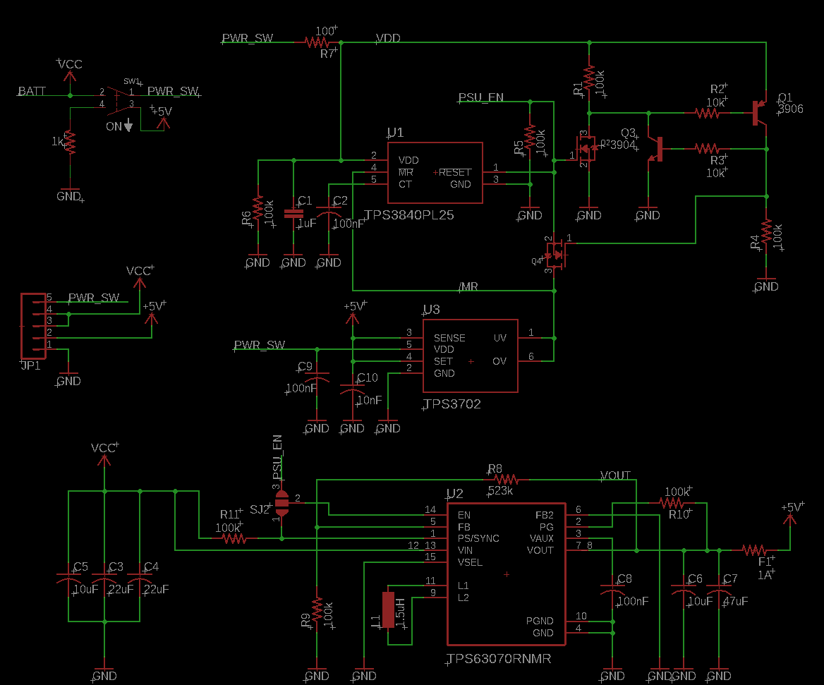
In this schematic, VCC is the voltage directly off of the batteries. When the batteries are inserted, the buck-boost is disabled initially (SJ2 is normally soldered so EN pin is connected to PSU_EN, these jumpers were added for troubleshooting purposes). Once the switch is turned on (SW1), battery voltage is applied to the TPS3840, and the /RESET line is pulled high once the power-on threshold is reached, which turns on the buck-boost. (Note: R7/C1 is added glitch protection during the start-up sequence of some downstream loads to prevent a false latch-off).
First question: In order to add the 5V window monitoring, my idea was to pull the /MR line on the TPS3840 low with the UV and OV outputs on a TPS3702 when the 5V line goes out of regulation (or when a user puts in wrong values for the feedback resistors and forgets to check the output before populating the rest of the assembly). The UV and OV pins should be pulled up, according to the TPS3702 datasheet, but the /MR pin has an internal 100k pull-up so I was going to rely on that. And I believe pulling /MR low in a 5V line error state would enable the latching circuit, ultimately turning the TPS63070 off until the power switch is cycled to reset the latch.
Is this strategy valid, and will the TPS3702 be able to fully pull the /MR line to GND during an error state if /RESET is still at VDD? Do I have to worry about conduction through Q4 body diode momentarily while OV pulls low and /RESET is still at VDD? Are there any flaws to this method, or is there a more reliable/efficient way of achieving the lockout?
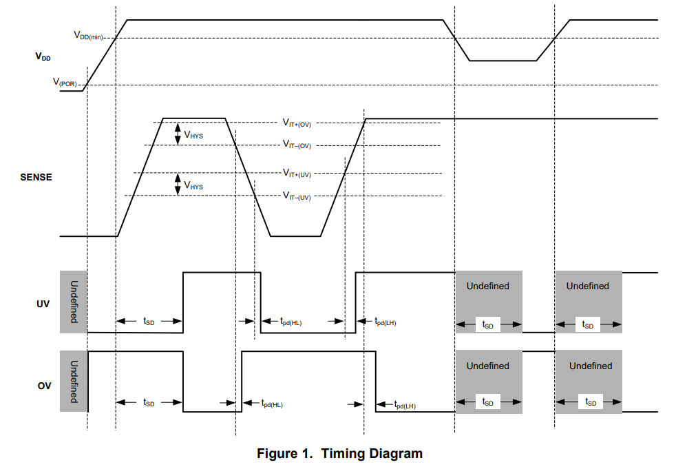
Second question: The TPS3702 has a startup delay of 300 microseconds. But when does this delay time start? Figure 1 in the datasheet seems to imply it's after VDD(min) is reached? Or is it related to the SENSE pin? I currently have a 100nF capacitor on the CT pin of the TPS3840 to delay enabling the TPS63070 by approximately 60 milliseconds after the power switch is turned on. So if VDD on the TPS3702 passes VDD(min), will the undervoltage sense automatically trigger? If necessary, I can remove the UV pin connection, since I am more concerned with overvoltage protection on the 5V line.
Thank you!