This thread has been locked.

If you have a related question, please click the "Ask a related question" button in the top right corner. The newly created question will be automatically linked to this question.

TPS23753A: How to fulfill the power up sequence and power down sequence of LM3881.

Part Number: TPS23753A
Other Parts Discussed in Thread: LM3881, LM3880

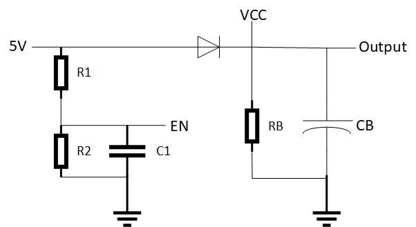
I want to input the output (+5.0V DC) of the TPS23257A to the VCC pin of the LM3881 to satisfy the power supply rising sequence and power supply falling sequence.

We have already confirmed that +5.0VDC can be output from the TPS23257A using the actual device from the circuit below.

We believe that +5.0V must be input to the VCC pin before the EN pin exceeds the Threshold Level (+1.22V) to satisfy the power rise sequence of the LM3881.

The datasheet states that the rise of the EN pin can be delayed by connecting an external capacitor to the EN pin.

Is it possible to meet the power rise sequence here?

We believe that in order to satisfy the power supply fall sequence of the LM3881, the voltage must be held long enough to allow enough time for the EN pin of the LM3881 to go LOW.

We believe we should add an external capacitor to hold the voltage, where should we add it?

Also, is there any other way to satisfy the power supply falling sequence?

  • Hello Kanta,

    To clarify, in your design, you want the EN pin to trigger from the output voltage from the TPS23257A, not an external trigger?

    Thanks,

    Broughton

  • Hello Broughton,

    That is correct.

    I want to operate the EN pin of the LM3881 by triggering the output voltage from the TPS23257A.

  • Hello Kanta,

    After looking into this for a while I've come up with two options.

    The first is taken from the LM3880 data sheet here (see Figure 8-5 on page 16): https://www.ti.com/lit/ds/symlink/lm3880.pdf. This shows a solution for configuring the Power-up sequencing from the same input voltage signal. However, if you want to configure both Power-up and Power-down sequencing it requires an independent external signal. Therefore, according to this data sheet, you can only meet Power-up sequencing requirements.

    The second option is a design I developed:


    Rise Sequence: The resistor network R1/R2 is just a voltage divider that should be set to the EN threshold voltage. The C1 capacitor is probably not necessary for this but I included it anyway. This resistor network will keep EN low until VCC is high enough to turn on the IC. 

    Fall Sequence: When 5V goes low, the EN pin will drop to low immediately as well. The bulk capacitor (CB) will then need to be large enough to supply the LM3881 along with whatever else is on the load for the 25 clock cycles necessary for the fall sequence. The diode will isolate the EN pin from the bulk capacitor. The bleeder resistor (RB) will need to be a relatively high resistance value. 

    A concern I have is that the bulk capacitor (or possibly multiple capacitors in series) may end up being quite large once you do the required calculations for the capacitance value. This design is by no means guaranteed to work.

    Let me know if you have any further questions!

    Thanks,

    Broughton

  • Hello Broughton,

    Thank you for your response.

    How many capacitor capacitances(CB) are required to meet the power down sequence?
    I would appreciate it if you could also tell me how to calculate this.

    Also, the power down sequence requires 40 clock cycles to be supplied; why is 40 clock cycles necessary?
    Is the time for the EN pin to fall in addition to the time for the FLAG1 pin (Td4), FLAG2 pin (Td5), and FLAG3 pin (Td6) to all fall?

  • Hello Kanta,

    I was incorrect about the 40 clock cycles. After looking at the data sheet, it is actually 25 clock cycles (9 + 8 + 8). Worst case scenario is 26 depending on where EN is asserted relative to the clock signal. Sorry about the confusion there.

    I am attempting to run a simulation of my proposed solution above but am encountering some issues during start-up while the capacitor is charging. I will update you on this as quickly as I can but I don't know if its possible to meet both power-up and power-down sequencing without an external signal. 

    Thanks,

    Broughton

  • Hello Kanta,

    If you decide to use a hold-up cap, there are some considerations to keep in mind. During startup when the cap is initialing charging, the PD may crash and it is likely to take multiple handshakes before the cap is fully charged. This will delay starting up significantly.

    To calculate the capacitance needed use I = C * dv/dt. Where dt is the necessary hold time and dv the allowable voltage drop over that time frame.

    I would recommend using an external signal if possible as meeting power-up and power-down sequencing requirements without an external signal is not advised or supported.

    Thanks,

    Broughton