


Hi,
Please could you give me some feedback on the following design.
TPS54394
1V1 @ 3A
1V5 @ 3A
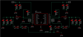
Most parts have their ratings on the schematic.
L1 & L2 = ABRACON ASPI-6045T-2R2N-T
Here's the layout:
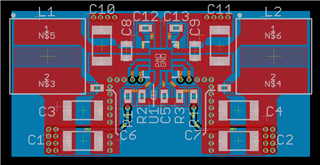
There are internal layers that are not shown, but these are solid GND pours. Should I relieve GND pours under the inductors? I've seen conflicting recommendations.
I've split the 5V inputs so they don't share the input capacitors, each input has it's own capacitors. Is that a good idea or should I just pour it all?
I would have liked the high frequency filter input capacitors closer to the input pins, but then they won't be connected to the top GND pour. Do they look ok where they are?
I'm a bit nervous about the width of the pour from the switching node, under the input caps, to the inductor. But I think this gives the best compromise? Thoughts?
Many thanks,
G

